Datasheet Summary
DATA SHEET
MOS INTEGRATED CIRCUIT
µPD16334
96-Bit AC-PDP DRIVER
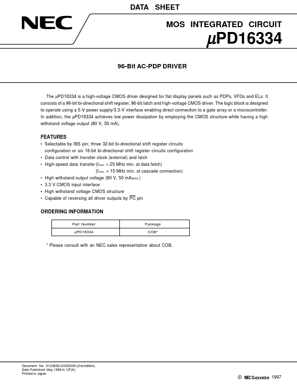
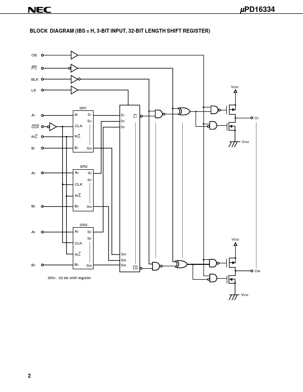
The µPD16334 is a high-voltage CMOS driver designed for flat display panels such as PDPs, VFDs and ELs. It consists of a 96-bit bi-directional shift register, 96-bit latch and high-voltage CMOS driver. The logic block is designed to operate using a 5-V power supply/3.3-V interface enabling direct connection to a gate array or a microcontroller. In addition, the µPD16334 achieves low power dissipation by employing the CMOS structure while having a high withstand voltage output (80 V, 50 mA).
Features
- Selectable by IBS pin; three 32-bit bi-directional shift register circuits configuration or six 16-bit bi-directional...