Datasheet Summary
DATA SHEET
MOS INTEGRATED CIRCUIT
µPD16337
64-BIT AC-PDP DRIVER
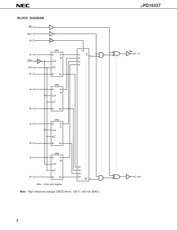
The µPD16337 is a high-voltage CMOS driver designed for flat display panels such as PDPs, VFDs and ELs. It consists of a 64-bit bi-directional shift register (16 bit × 4 circuits), 64-bit latch and high-voltage CMOS driver. The logic block is designed to operate at 5-V power supply, enabling direct connection to a microcontroller. In addition, the µPD16337 achieves low power dissipation by employing CMOS structure while having a high withstand voltage output (150 V, 40 mA MAX.)
Features
- Built in four 16-bit bi-directional shift register circuits
- Data control with transfer clock (external) and latch
- High-speed data...