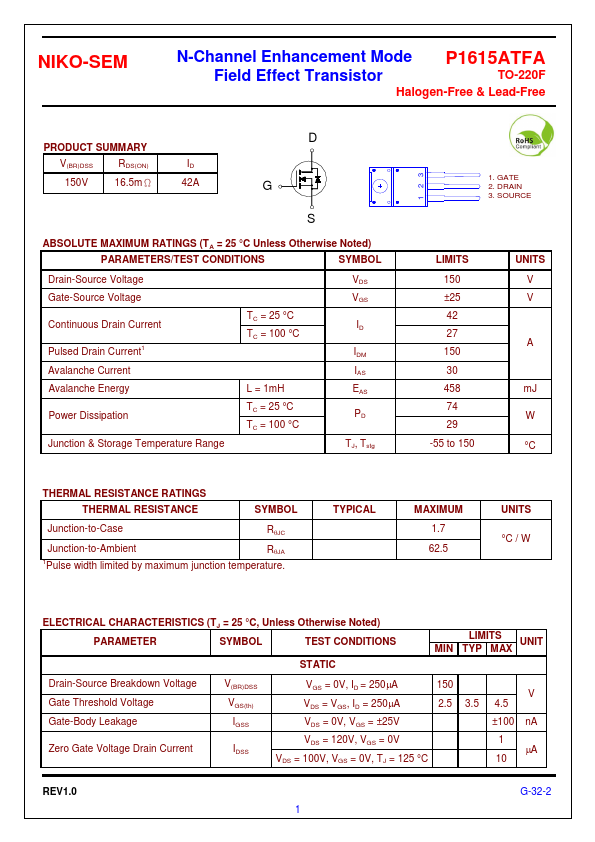
Download the P1615ATFA datasheet PDF.
This datasheet also covers the P1615ATFA-NIKO variant, as both devices belong to the same n-channel transistor family and are provided as variant models within a single manufacturer datasheet.
Full PDF Text Transcription for P1615ATFA (Reference)
Note: Below is a high-fidelity text extraction (approx. 800 characters) for
P1615ATFA. For precise diagrams, and layout, please refer to the original PDF.
NIKO-SEM N-Channel Enhancement Mode P1615ATFA Field Effect Transistor TO-220F Halogen-Free & Lead-Free PRODUCT SUMMARY V(BR)DSS RDS(ON) 150V 16.5mΩ ID 42A D G S ABSOLUTE ...
View more extracted text
ee PRODUCT SUMMARY V(BR)DSS RDS(ON) 150V 16.5mΩ ID 42A D G S ABSOLUTE MAXIMUM RATINGS (TA = 25 °C Unless Otherwise Noted) PARAMETERS/TEST CONDITIONS SYMBOL Drain-Source Voltage Gate-Source Voltage Continuous Drain Current Pulsed Drain Current1 Avalanche Current Avalanche Energy Power Dissipation Junction & Storage Temperature Range TC = 25 °C TC = 100 °C L = 1mH TC = 25 °C TC = 100 °C VDS VGS ID IDM IAS EAS PD TJ, Tstg 1 23 1. GATE 2. DRAIN 3.