P5506BDA Overview
| Part | P5506BDA |
|---|---|
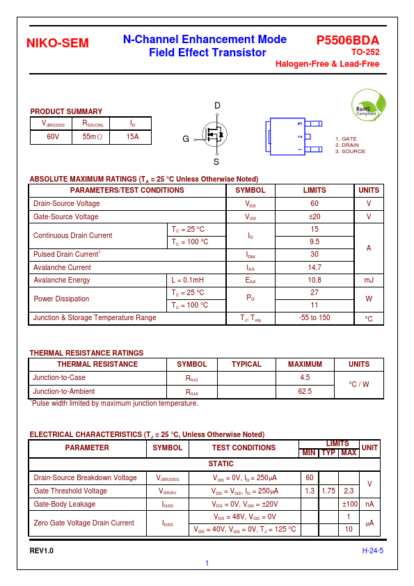
| Description | N-Channel Enhancement Mode Field Effect Transistor |
| Category | Transistor |
| Manufacturer | NIKO-SEM |
| Size | 215.00 KB |
| Part Number | Manufacturer | Description |
|---|---|---|
| P5506BDA | Inchange Semiconductor | N-Channel MOSFET |
| P5506BDG | Niko | N-Channel MOSFET |
| P5506BDG | UNIKC | N-Channel MOSFET |
| P5506BVG | UNIKC | N-Channel MOSFET |
| P5506BVG | Niko | N-Channel Logic Level Enhancement Mode Field Effect Transistor |