P9006EDA Overview
Key Features
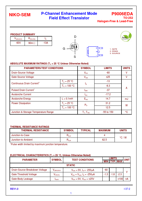
- 1.3 -1.8 -2.3
| Part | P9006EDA |
|---|---|
| Description | P-Channel Enhancement Mode Field Effect Transistor |
| Category | Transistor |
| Manufacturer | NIKO-SEM |
| Size | 210.83 KB |
| Part Number | Manufacturer | Description |
|---|---|---|
| P9006EDG | VBsemi | P-Channel MOSFET |
| P9006EDG | UNIKC | P-Channel MOSFET |
| P9006EVG | UNIKC | P-Channel MOSFET |
| P9006ETF | UNIKC | P-Channel MOSFET |
| P9006EI | UNIKC | P-Channel MOSFET |