NXP Semiconductors BF909R
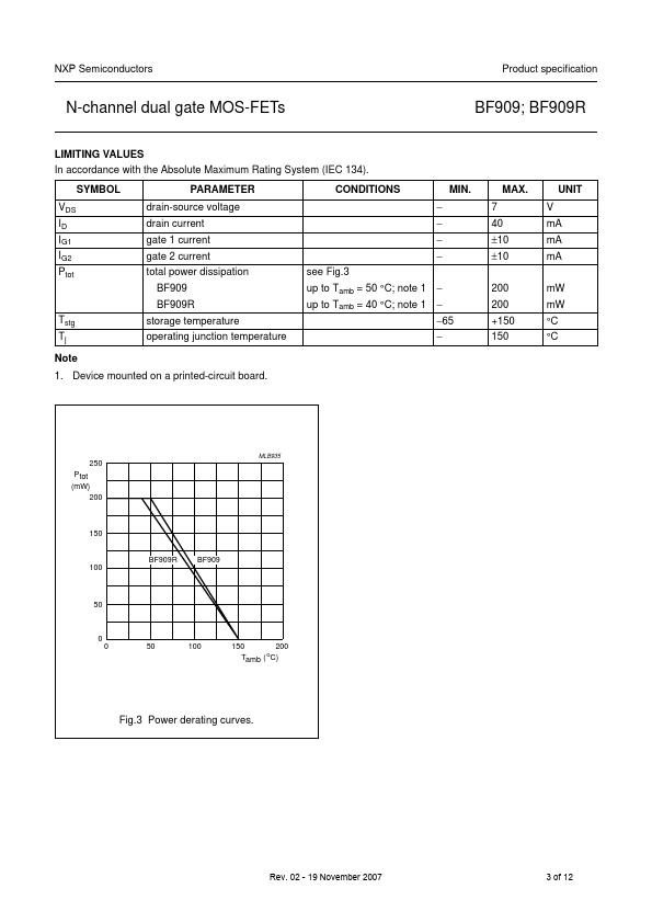
The PINNING PIN 1 2 3 4 SYMBOL DESCRIPTION s, b source d drain g2 gate 2 g1 gate 1 handbook, halfpage d handbook, halfpage d 4 3 3 4 g2 g1 1 2 Top view MAM124 s,b BF909 marking code: %M3.| Part No. | BF909R |
|---|---|
| Datasheet | BF909R Download |
| Manufacturer |  NXP Semiconductors |
| Description | N-channel dual gate MOS-FET |
| Buy | Stock & Price |
FEATURES
● Specially designed for use at 5 V supply voltage● High forward transfer admittance
● Short channel transistor with high forward transfer admittance to input capacitance ratio
● Low noise gain controlled amplifier up to 1 GHz
● Superior cross-modulation performance during AGC. transistor consists of an amplifier MOS-FET with source and substrate interconnected and an internal bias circuit to ensure good cross-modulation performance during AGC. CAUTION The device is supplied in an antistatic package. The gate-source input must be protected against static discharge during transport or handling.
APPLICATIONS
● VHF and UHF applications with 3 to 7 V supply voltage such as television tuners and professional communications equipment.DESCRIPTION
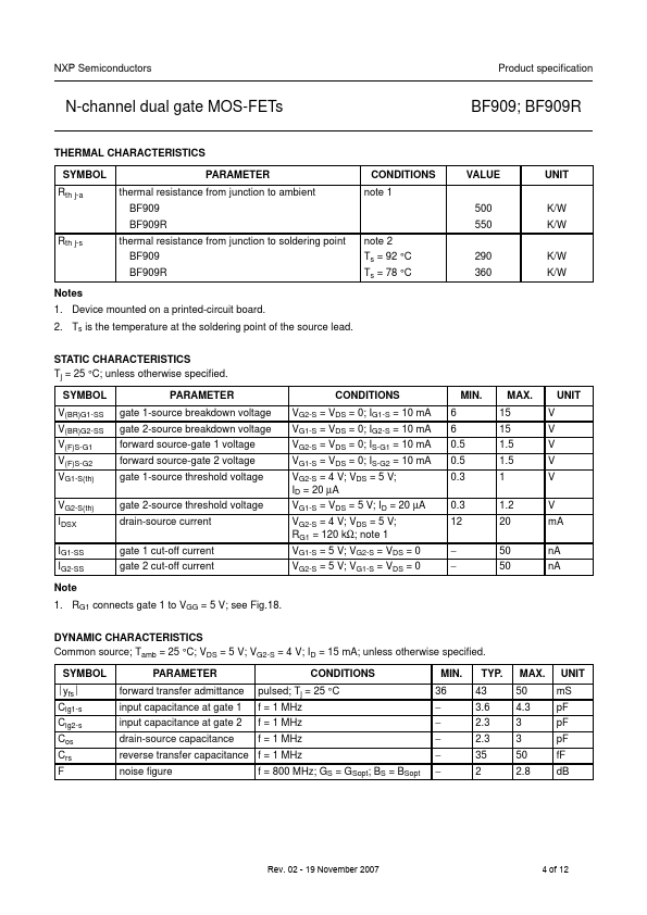
Enhancement type field-effect transistor in a plastic microminiature SOT143 or SOT143R package. Fig.1 Simplified outline (SOT143) and symbol. g2 g1 21 Top view MAM125 - 1 s,b BF909R marking code: %M4. Fig.2 Simplified outline (SOT143R) and symbol.