NXP Semiconductors CGY2014
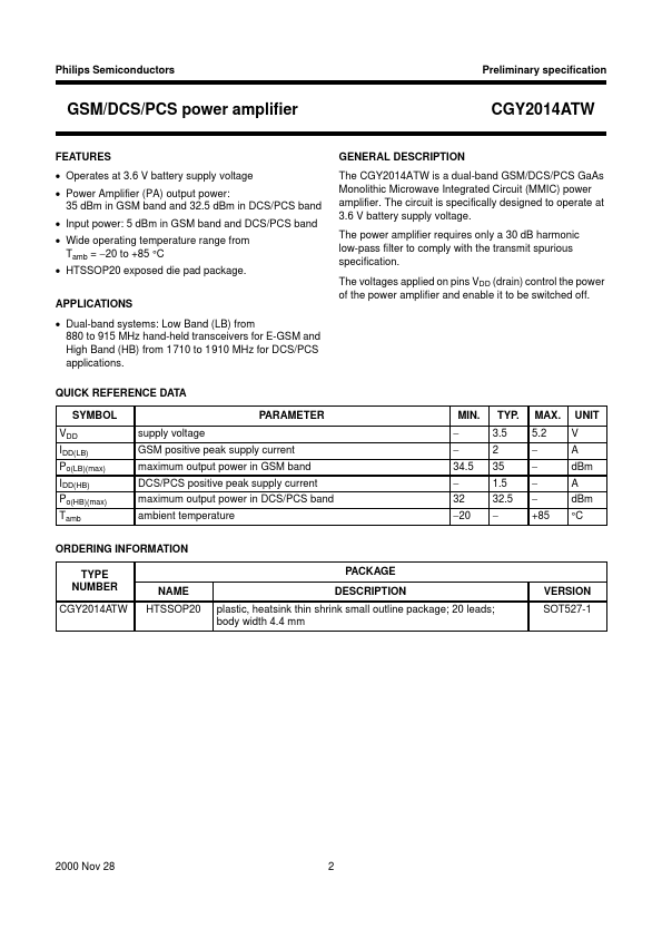
The CGY2014ATW is a dual-band GSM/DCS/PCS GaAs Monolithic Microwave Integrated Circuit (MMIC) power amplifier. The circuit is specifically designed to operate at 3.6 V battery supply voltage. The power amplifier requires only a 30 dB harmonic low-pass filter to comply with the transmit spurious specification.| Part No. | CGY2014 |
|---|---|
| Datasheet | CGY2014 Download |
| Manufacturer |  NXP Semiconductors |
| Description | GSM/DCS/PCS power amplifier |
| Buy | Stock & Price |

FEATURES
● Operates at 3.6 V battery supply voltage● Power Amplifier (PA) output power: 35 dBm in GSM band and 32.5 dBm in DCS/PCS band
● Input power: 5 dBm in GSM band and DCS/PCS band
● Wide operating temperature range from Tamb = −20 to +85 °C
● HTSSOP20 exposed die pad package.
APPLICATIONS
● Dual-band systems: Low Band (LB) from 880 to 915 MHz hand-held transceivers for E-GSM and High Band (HB) from 1710 to 1910 MHz for DCS/PCS applications. QUICK REFERENCE DATA SYMBOL VDD IDD(LB) Po(LB)(max) IDD(HB) Po(HB)(max) Tamb supply voltage GSM positive peak supply current maximum output power in GSM band DCS/PCS positive peak supply current maximum output power in DCS/PCS band ambient temperature PARAMETER MIN. − − 34.5 − 32 −20GENERAL DESCRIPTION
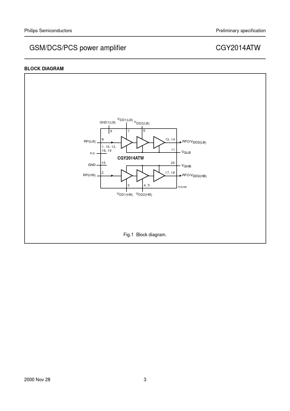
CGY2014ATW The voltages applied on pins VDD (drain) control the power of the power amplifier and enable it to be switched off. TYP. 3.5 2 35 1.5 32.5 − MAX. 5.2 − − − − +85 UNIT V A dBm A dBm °C ORDERING INFORMATION TYPE NUMBER CGY2014ATW PACK...