PDTA114ES
FEATURES
- Built-in bias resistors R1 and R2 (typ. 10 kΩ each)
- Simplification of circuit design
- Reduces number of ponents and board space. APPLICATIONS
- Especially suitable for space reduction in interface and driver circuit applications
- Inverter circuit configurations without use of external resistors. DESCRIPTION
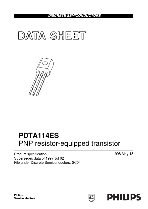
PNP resistor-equipped transistor in a TO-92; SOT54 plastic package. NPN plement: PDTC114ES. PINNING PIN 1 2 3 DESCRIPTION base/input collector/output emitter/ground (+) Fig.2 Equivalent inverter symbol.
MAM338
PDTA114ES handbook, halfpage
2 R1 1 R2 3
1 2 3
Fig.1 Simplified outline (TO-92; SOT54) and symbol.
1 3
MGL136
QUICK REFERENCE DATA SYMBOL VCEO IO ICM Ptot h FE R1 R2 ------R1 PARAMETER collector-emitter voltage output current (DC) peak collector current total power dissipation DC current gain input resistor resistor ratio Tamb ≤ 25 °C IC =
- 5 m A; VCE =
- 5 V CONDITIONS open base
- -
- - 30 7 0.8 MIN.
- -
- -
- 10 1 TYP. MAX.
- 50
- 100
- 100 500
- 13 1.2...