PHB2N50
PHB2N50 is PowerMOS transistor manufactured by NXP Semiconductors.
DESCRIPTION
N-channel enhancement mode field-effect power transistor in a plastic envelope suitable for surface mounting featuring high avalanche energy capability, stable off-state characteristics, fast switching and high thermal cycling performance with low thermal resistance. Intended for use in Switched Mode Power Supplies (SMPS), motor control circuits and general purpose switching applications.
QUICK REFERENCE DATA
SYMBOL VDS ID Ptot RDS(ON) PARAMETER Drain-source voltage Drain current (DC) Total power dissipation Drain-source on-state resistance MAX. 500 2 50 5 UNIT V A W Ω
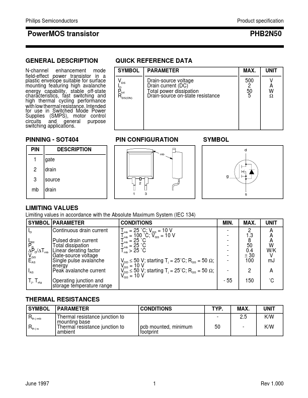
PINNING
- SOT404
PIN 1 2 3 mb gate drain source drain DESCRIPTION
PIN CONFIGURATION mb
SYMBOL d g
2 1 3 s
LIMITING VALUES
Limiting values in accordance with the Absolute Maximum System (IEC 134) SYMBOL PARAMETER ID IDM PD ∆PD/∆Tmb VGS EAS IAS Tj, Tstg Continuous drain current Pulsed drain current Total dissipation Linear derating factor Gate-source voltage Single pulse avalanche energy Peak avalanche current Operating junction and storage temperature range CONDITIONS Tmb = 25 ˚C; VGS = 10 V Tmb = 100 ˚C; VGS = 10 V Tmb = 25 ˚C Tmb = 25 ˚C Tmb > 25 ˚C VDD ≤ 50 V; starting Tj = 25˚C; RGS = 50 Ω; VGS = 10 V VDD ≤ 50 V; starting Tj = 25˚C; RGS = 50 Ω; VGS = 10 V MIN.
- 55 MAX. 2 1.3 8 50 0.4 ± 30 100 2 150 UNIT A A A W W/K V m J A ˚C
THERMAL RESISTANCES
SYMBOL Rth j-mb Rth j-a PARAMETER Thermal resistance junction to mounting base Thermal resistance junction to ambient CONDITIONS TYP. pcb mounted, minimum footprint 50 MAX. 2.5 UNIT K/W K/W
June 1997
Rev 1.000
Philips Semiconductors
Product specification
Power MOS transistor
ELECTRICAL CHARACTERISTICS
Tj = 25 ˚C unless otherwise specified SYMBOL V(BR)DSS ∆V(BR)DSS / ∆Tj RDS(ON) VGS(TO) gfs IDSS IGSS Qg(tot) Qgs Qgd td(on) tr td(off) tf Ld Ld Ls Ciss Coss Crss PARAMETER Drain-source breakdown voltage Drain-source breakdown voltage temperature coefficient Drain-source on resistance Gate threshold voltage Forward...