NXP Semiconductors SC18IS601
the SC18IS601 lies in the clock source: internal (SC18IS600) versus external (SC18IS601).| Part No. | SC18IS601 |
|---|---|
| Datasheet | SC18IS601 Download |
| Manufacturer |  NXP Semiconductors |
| Description | SPI to IC-bus interface |
| Buy | Stock & Price |
FEATURES
I I I I I I I SPI slave interface SPI Mode 3 Master I2C-bus controller General Purpose Input/Output (GPIO) pins: 4 (SC18IS600); 3 (SC18IS601) Two quasi-bidirectional I/O pins 5 V tolerant I/O pins High-speed SPI: N Up to 3 Mbit/s (SC18IS601) N Up to 1.2 Mbit/s (SC18IS600) High-speed I2C-bus: 400 kbit/s 96-byte transmit buffer 96-byte receive buffer 2.4 V to 3.6 V operation Power-down mode with WAKEUP pin Oscillator: internal (SC18IS600); external (SC18IS601) Active LOW interrupt output Available in very small TSSOP16 package I I I I I I I I 3. Ordering information Table 1. Ordering information Package Name SC18IS600IPW SC18IS601IPW TSSOP16DESCRIPTION
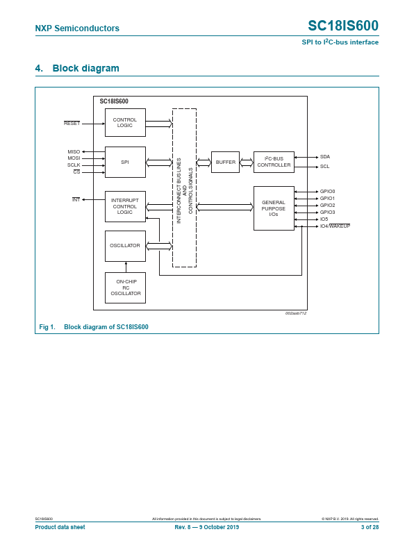
plastic thin shrink small outline package; 16 leads; body width 4.4 mm Version SOT403-1 Type number NXP Semiconductors SC18IS600/601 SPI to I2C-bus interface 4. Block diagram SC18IS600 CONTROL LOGIC RESET INTERCONNECT BUS LINES AND CONTROL SIGNALS MISO MOSI SCLK CS SPI BUFFER I2C-BUS CONTROLLER SDA SCL INT INTERRUPT CONTROL LOGIC GENERAL PURPOSE I/Os GPIO0 GPIO1 GPIO2 GPIO3 IO5 IO4/WAKEUP OSCILLATOR ON-CHIP RC OSCILLATOR 002aab712 Fig 1.