CGS701TV
CGS701TV is Low Skew PLL 1 to 8 CMOS Clock Driver manufactured by National Semiconductor.
- Part of the CGS701V comparator family.
- Part of the CGS701V comparator family.
Description
CGS701 is an off the shelf clock driver specifically designed for today's high speed designs. It provides low skew outputs which are produced at different frequencies from three fixed input references. The XTALIN input pin is designed to be driven from a 15 MHz-50 MHz crystal oscillator.
The PLL, using a charge pump and an internal loop filter, multiplies this input frequency to create a maximum output frequency of four times the input.
The device includes a TRI-STATE® control pin to disable the outputs. This feature allows for low frequency functional testing and debugging.
Also included, is an EXTSEL pin to allow testing the chip via an external source. The EXTSEL pin, once set to high, caus- es the External-Cloc LMUX to change its input from the output of the VCO and Counter to the external clock signal provided via SKWTST input pin.
(continued)
Features
- Guaranteed and tested: 500 ps pin-to-pin skew (t OSHL and t OSLH) on 1X out- puts. ± 500 ps propagation delay
- Output buffer of eight drivers for large fanout
- 25 MHz-160 MHz output frequency range
- Outputs operating at 4X, 2X, 1X of the reference frequency for multifrequency bus applications
- Selectable output frequency
- Internal loop filter to reduce noise and jitter
- Separate analog and digital Vee and ground pins
- Low frequency test mode by disabling the PLL
- Implemented on National's Core CMOS process
- Symmetric output current drive: + 30/
- 30 m A IOLli OH
- Industrial temperature of -40'C to + 85'C
- 28-pin pce for optimum skew performance
- Guaranteed 2 k V ESD protection
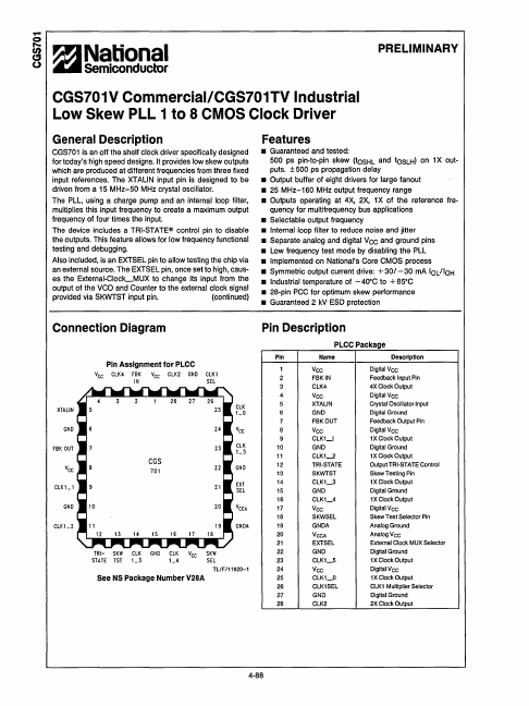
Connection Diagram
Pin Assignment for PLCC vee Cl K4 r SK vee Cl K2 GND Cl Kl
SEl
XIALIN GND r BK OUT Vee
Cl KLl GND
CLKL2
Cl K LO
Vee
Cl K L5
EXT SEl
Vee A
GNDA
TRI- SKW Cl K GND Cl K Vee SKW
STAl E 1ST L3
L4
SEl
TL/F/11920-1...