3LP01SS
3LP01SS is P-Channel Small Signal MOSFET manufactured by onsemi.
Features
- Low ON-resistance
- High-speed switching
- 2.5V drive
Specifications
Absolute Maximum Ratings at Ta=25°C
Parameter
Symbol
Conditions
Drain-to-Source Voltage Gate-to-Source Voltage Drain Current (DC) Drain Current (Pulse) Allowable Power Dissipation Channel Temperature
VDSS VGSS ID IDP PD Tch
PW≤10μs, duty cycle≤1%
Storage Temperature
Tstg
This product is designed to “ESD immunity < 200V- ”, so please take care when handling.
- Machine Model
Ratings --30 ±10 --0.1 --0.4 0.15 150
--55 to +150
Unit V V A A W °C °C
Stresses exceeding Maximum Ratings may damage the device. Maximum Ratings are stress ratings only. Functional operation above the Remended Operating Conditions is not implied. Extended exposure to stresses above the Remended Operating Conditions may affect device reliability.
LOT No. LOT No.
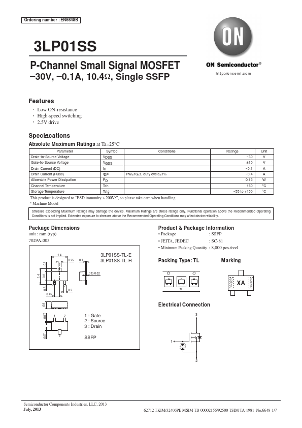
Package Dimensions unit : mm (typ) 7029A-003
1.4 0.3 0.8 0.3
1.4 0.25 0.1
3LP01SS-TL-E 3LP01SS-TL-H
0 to 0.02
1 0.45
2 0.2
0.07 0.6
12 3
1 : Gate 2 : Source 3 : Drain
SSFP
Product & Package Information
- Package
: SSFP
- JEITA, JEDEC
: SC-81
- Minimum Packing Quantity : 8,000...