ATP401
ATP401 is N-Channel Power MOSFET manufactured by onsemi.
Ordering number : ENA2167
N-Channel Power MOSFET
60V, 100A, 3.7mΩ, ATPAK http://onsemi.
Features
- ON-resistance RDS(on)1=2.8mΩ(typ)
- 4.5V Drive
- Input Capasitance Ciss=17000p F(typ)
- Halogen free pliance
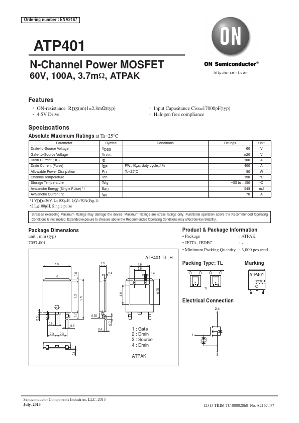
Specifications...