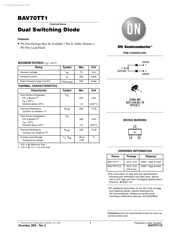
BAV70TT1
Overview
- Pb-Free Package May be Available.* The G-Suffix Denotes a Pb-Free Lead Finish
| Part Number | Manufacturer | Description |
|---|---|---|
| BAV70T | Formosa MS | SMD Small Signal Switching Diode |
| BAV70T | Semiware Semiconductor | Surface Mount Fast Switching Doide |
| BAV70T | Fairchild Semiconductor | Fast Switching Diode |
| BAV70T | Infineon | Silicon Switching Diode |
| BAV70T | KEC | SILICON EPITAXIAL PLANAR DIODE |