FDMA1027P
Overview
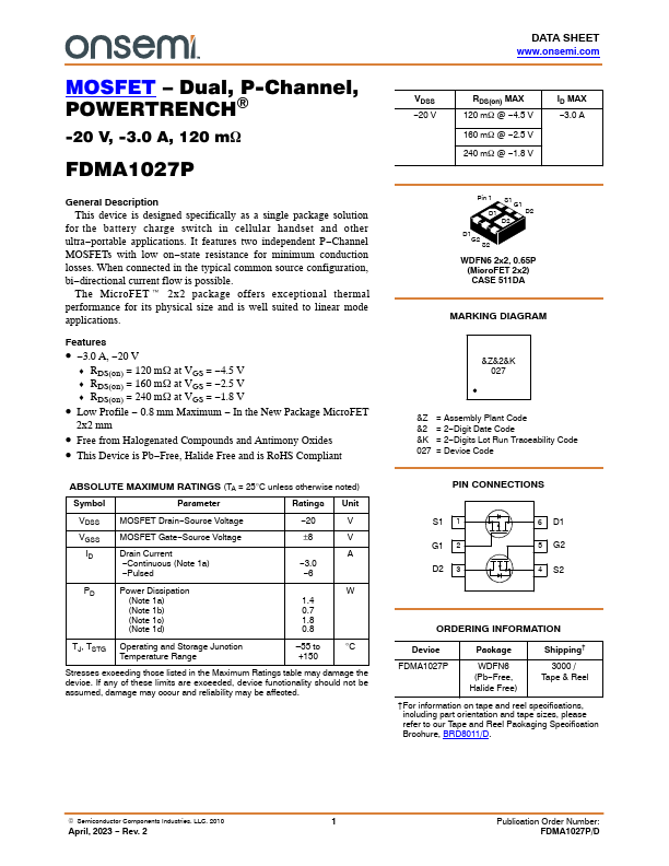
This device is designed specifically as a single package solution for the battery charge switch in cellular handset and other ultra-portable applications. It features two independent P-Channel MOSFETs with low on-state resistance for minimum conduction losses.
- -3.0 A, -20 V
- RDS(on) = 120 mW at VGS = -4.5 V
- RDS(on) = 160 mW at VGS = -2.5 V
- RDS(on) = 240 mW at VGS = -1.8 V
- Low Profile - 0.8 mm Maximum - In the New Package MicroFET 2x2 mm
- Free from Halogenated Compounds and Antimony Oxides
- This Device is Pb-Free, Halide Free and is RoHS Compliant