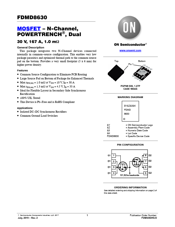
FDMD8630 Description
This package integrates two N−Channel devices connected internally in mon−source configuration. This enables very low package parasitics and optimized thermal path to the mon source pad on the bottom. Provides a very small footprint (5 x 6 mm) for higher power density.
FDMD8630 Key Features
- mon Source Configuration to Eliminate PCB Routing
- Large Source Pad on Bottom of Package for Enhanced Thermals
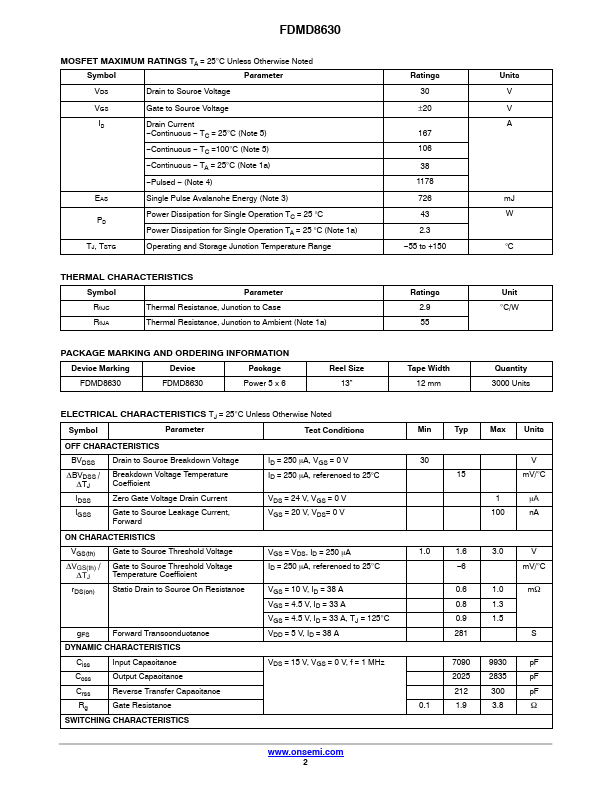
- Max rDS(on) = 1.0 mW at VGS = 10 V, ID = 38 A
- Max rDS(on) = 1.3 mW at VGS = 4.5 V, ID = 33 A
- Ideal for Flexible Layout in Secondary Side Synchronous
- 100% UIL Tested
- This Device is Pb-Free and is RoHS pliant