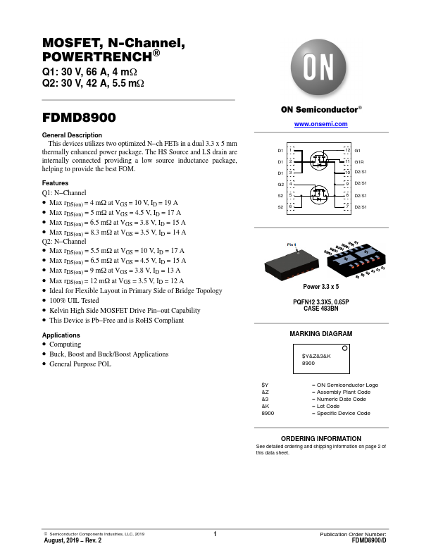
FDMD8900 Description
This devices utilizes two optimized N−ch FETs in a dual 3.3 x 5 mm thermally enhanced power package. The HS Source and LS drain are internally connected providing a low source inductance package, helping to provide the best FOM.
FDMD8900 Key Features
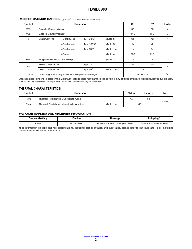
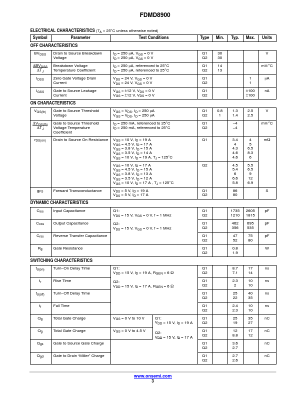
- Max rDS(on) = 4 mW at VGS = 10 V, ID = 19 A
- Max rDS(on) = 5 mW at VGS = 4.5 V, ID = 17 A
- Max rDS(on) = 6.5 mW at VGS = 3.8 V, ID = 15 A
- Max rDS(on) = 8.3 mW at VGS = 3.5 V, ID = 14 A
- Max rDS(on) = 5.5 mW at VGS = 10 V, ID = 17 A
- Max rDS(on) = 6.5 mW at VGS = 4.5 V, ID = 15 A
- Max rDS(on) = 9 mW at VGS = 3.8 V, ID = 13 A
- Max rDS(on) = 12 mW at VGS = 3.5 V, ID = 12 A
- Ideal for Flexible Layout in Primary Side of Bridge Topology
- 100% UIL Tested