FDMS3669S
Description
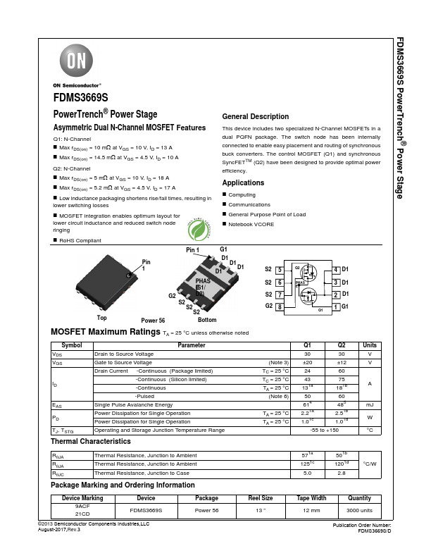
Asymmetric Dual N-Channel MOSFET Features Q1: N-Channel - Max rDS(on) = 10 mΩ at VGS = 10 V, ID = 13 A - Max rDS(on) = 14.5 mΩ at VGS = 4.5 V, ID = 10 A Q2: N-Channel - Max rDS(on) = 5 mΩ at VGS = 10 V, ID = 18 A - Max rDS(on) = 5.2 mΩ at VGS = 4.5 V, ID = 17 A - Low inductance packaging shortens rise/fall times, resulting in lower switching losses - MOSFET integration enables optimum layout for lower circuit inductance and reduced switch node ringing This device includes two specialized N-Channel MOSFETs in a dual PQFN package.
Key Features
- Q1: N-Channel
- Max rDS(on) = 10 mΩ at VGS = 10 V, ID = 13 A
- Max rDS(on) = 14.5 mΩ at VGS = 4.5 V, ID = 10 A Q2: N-Channel
- Max rDS(on) = 5 mΩ at VGS = 10 V, ID = 18 A
- Max rDS(on) = 5.2 mΩ at VGS = 4.5 V, ID = 17 A
- Low inductance packaging shortens rise/fall times, resulting in lower switching losses


