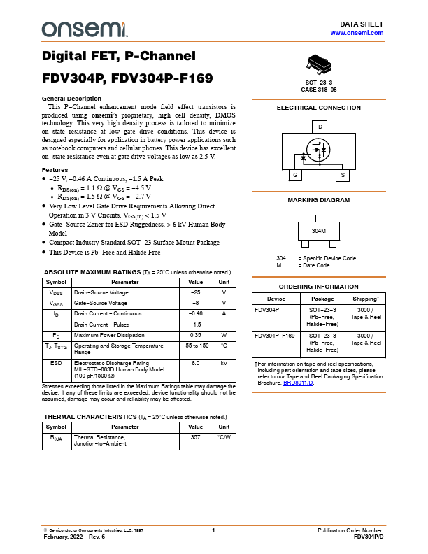
FDV304P
Description
This P- Channel enhancement mode field effect transistors is produced using onsemi’s proprietary, high cell density, DMOS technology. This very high density process is tailored to minimize on- state resistance at low gate drive conditions. This device is designed especially for application in battery power applications such as notebook puters and cellular phones. This device has excellent on- state resistance even at gate drive voltages as low as 2.5 V.
Features
- - 25 V,
- 0.46 A Continuous,
- 1.5 A Peak
- RDS(on) = 1.1 W @ VGS =
- 4.5 V
- RDS(on) = 1.5 W @ VGS =
- 2.7 V
- Very Low Level Gate Drive Requirements Allowing Direct
Operation in 3 V Circuits. VGS(th) < 1.5 V
- Gate- Source Zener for ESD Ruggedness. > 6 k V Human Body
Model
- pact Industry Standard SOT- 23 Surface Mount Package
- This Device is Pb- Free and Halide Free
ABSOLUTE MAXIMUM RATINGS (TA = 25°C unless otherwise noted.)
Symbol
Parameter
Value
Unit
VDSS VGSS
Drain- Source Voltage Gate- Source Voltage Drain...