Datasheet4U Logo Datasheet4U.com

MC100EP196A - 3.3 V ECL Programmable Delay Chip

Datasheet Summary

Description

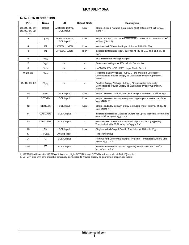
Pin Name I/O Default State Description 23, 25, 26, 27, D[0:9] LVCMOS, LVTTL, Low Single

Ended Parallel Data Inputs [0:9].

Internal 75 kW to VEE.

Features

  • Parameter Condition 1 Condition 2 Rating Unit VCC Positive Mode Power Supply VEE Negative Mode Power Supply VI Positive Mode Input Voltage Negative Mode Input Voltage Iout Output Current VEE = 0 V VCC = 0 V VEE = 0 V VCC = 0 V Continuous Surge VI ≤ VCC VI ≥ VEE 6V.
  • 6 V 6V.
  • 6 V 50 mA 100 mA IBB VBB Sink/Source TA Operating Temperature Range Tstg Sto.

📥 Download Datasheet

Datasheet preview – MC100EP196A

Datasheet Details

Part number MC100EP196A
Manufacturer ON Semiconductor
File Size 149.59 KB
Description 3.3 V ECL Programmable Delay Chip
Datasheet download datasheet MC100EP196A Datasheet
Additional preview pages of the MC100EP196A datasheet.
Other Datasheets by ON Semiconductor

Full PDF Text Transcription

Click to expand full text
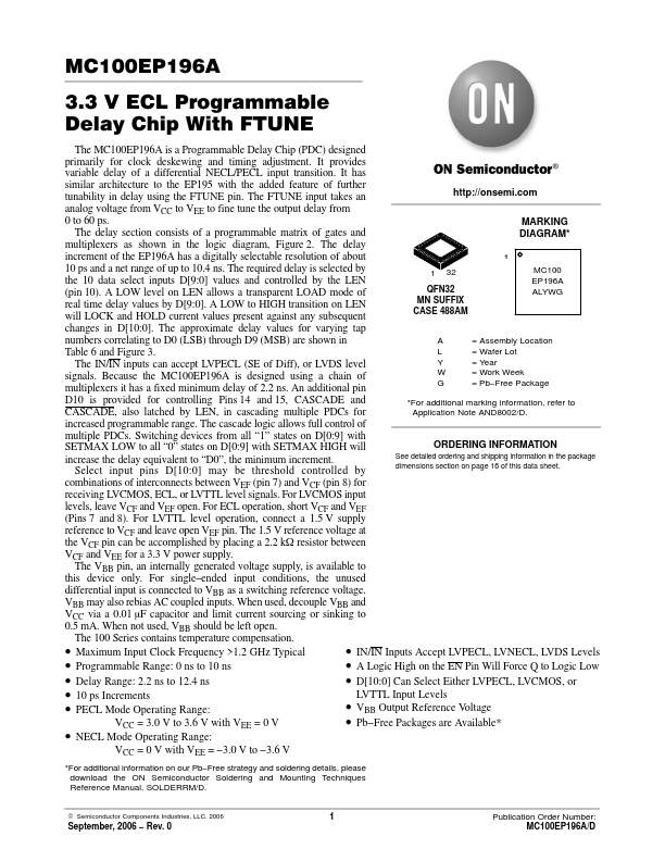
MC100EP196A 3.3 V ECL Programmable Delay Chip With FTUNE The MC100EP196A is a Programmable Delay Chip (PDC) designed primarily for clock deskewing and timing adjustment. It provides variable delay of a differential NECL/PECL input transition. It has similar architecture to the EP195 with the added feature of further tunability in delay using the FTUNE pin. The FTUNE input takes an http://onsemi.com analog voltage from VCC to VEE to fine tune the output delay from 0 to 60 ps. MARKING The delay section consists of a programmable matrix of gates and DIAGRAM* multiplexers as shown in the logic diagram, Figure 2. The delay increment of the EP196A has a digitally selectable resolution of about 1 10 ps and a net range of up to 10.4 ns.
Published: |