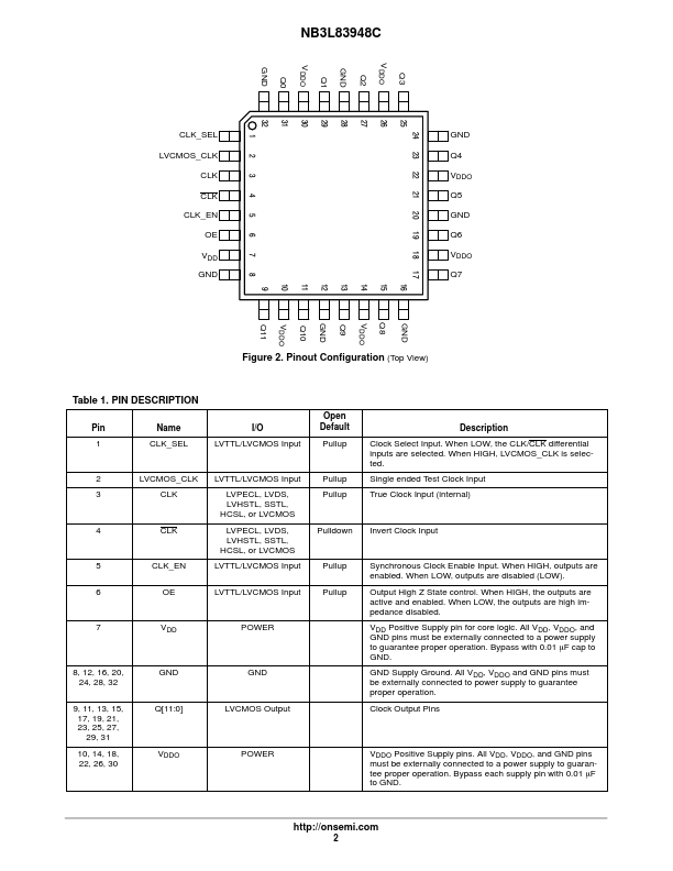
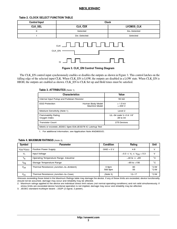
Datasheet Summary
2.5 V / 3.3 V Differential and LVTTL/LVCMOS 2:1 MUX to 1:12 LVCMOS Fanout
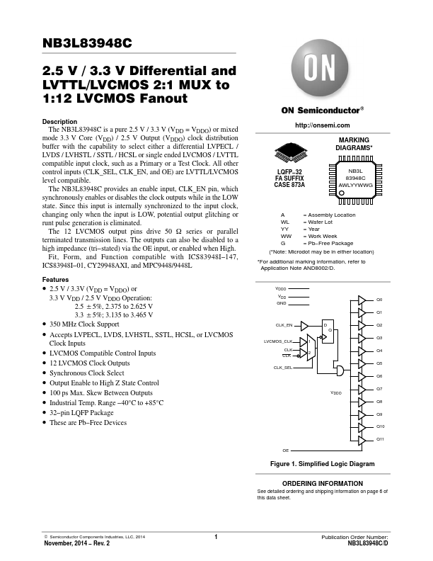
Description The NB3L83948C is a pure 2.5 V / 3.3 V (VDD = VDDO) or mixed mode 3.3 V Core (VDD) / 2.5 V Output (VDDO) clock distribution buffer with the capability to select either a differential LVPECL / LVDS / LVHSTL / SSTL / HCSL or single ended LVCMOS / LVTTL patible input clock, such as a Primary or a Test Clock. All other control inputs (CLK_SEL, CLK_EN, and OE) are LVTTL/LVCMOS level patible.
The NB3L83948C provides an enable input, CLK_EN pin, which synchronously enables or disables the clock outputs while in the LOW state. Since this input is internally synchronized to the input clock,...