Datasheet4U Logo Datasheet4U.com

NB3L8504S - 2.5V / 3.3V 1:4 Differential Input to LVDS Fanout Buffer / Translator

General Description

with OE control for each differential output.

ended input, can accept various logic level standards such as LVPECL, LVDS, HSTL, HCSL and SSTL.

Key Features

  • Four Differential LVDS Outputs.
  • Each Differential Output has OE Control.
  • 700 MHz Maximum Output Frequency.
  • 660 ps Max Output Rise and Fall Times, LVCMOS.
  • Translates Differential Input to LVDS Levels.
  • Additive Phase Jitter RMS: < 100 fs Typical.
  • 50 ps Maximum Output Skew.
  • 350 ps Maximum Part.
  • to.
  • part Skew.
  • 1.3 ns Maximum Propagation Delay.

📥 Download Datasheet

Datasheet Details

Part number NB3L8504S
Manufacturer onsemi
File Size 246.12 KB
Description 2.5V / 3.3V 1:4 Differential Input to LVDS Fanout Buffer / Translator
Datasheet download datasheet NB3L8504S Datasheet

Full PDF Text Transcription (Reference)

The following content is an automatically extracted verbatim text from the original manufacturer datasheet and is provided for reference purposes only.

View original datasheet text
NB3L8504S 2.5 V / 3.3 V 1:4 Differential Input to LVDS Fanout Buffer / Translator 
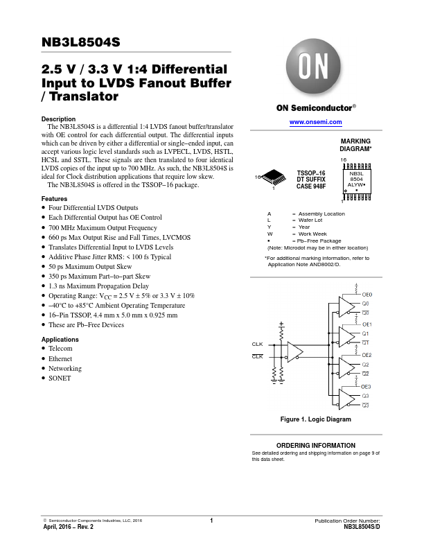
Description The NB3L8504S is a differential 1:4 LVDS fanout buffer/translator with OE control for each differential output. The differential inputs which can be driven by either a differential or single−ended input, can accept various logic level standards such as LVPECL, LVDS, HSTL, HCSL and SSTL. These signals are then translated to four identical LVDS copies of the input up to 700 MHz. As such, the NB3L8504S is ideal for Clock distribution applications that require low skew. The NB3L8504S is offered in the TSSOP−16 package.