NB3M8302C
NB3M8302C is 3.3V 200 MHz 1:2 LVCMOS/LVTTL Low Skew Fanout Buffer manufactured by onsemi.
3.3 V 200 MHz 1:2 LVCMOS/LVTTL Low Skew Fanout Buffer
Description The NB3M8302C is 1:2 fanout buffer with LVCMOS/LVTTL input and output. The device supports the core supply voltage of 3.3 V (VDD pin) and output supply voltage of 2.5 V or 3.3 V (VDDO pin). The VDDO pin powers the two single ended LVCMOS/LVTTL outputs.
The NB3M8302C is Form, Fit and Function (pin to pin) patible to ICS8302 and ICS8302I. The NB3M8302C is qualified for industrial operating temperature range.
Features
- Input Clock Frequency up to 200 MHz
- Low Output to Output Skew: 25 ps typical
- Low Part to Part Skew: 250 ps typical
- Low Additive RMS Phase Jitter
- Input Clock Accepts LVCMOS/ LVTTL Levels
- Operating Voltage:
- Core Supply: VDD = 3.3 V ±5%
- Output Supply: VDDO = 3.3 V ±5% or 2.5 V ±5%
- Operating Temperature Range:
- Industrial:
- 40°C to +85°C
- These Devices are Pb- Free and are Ro HS pliant
.onsemi.
1 SOIC- 8 D SUFFIX CASE 751
MARKING DIAGRAMS-
8302C ALYWG
G 1
A = Assembly Location L = Wafer Lot Y = Year W = Work Week G = Pb- Free Package
(Note: Microdot may be in either location)
ORDERING INFORMATION
See detailed ordering and shipping information in the package dimensions section on page 5 of this data sheet.
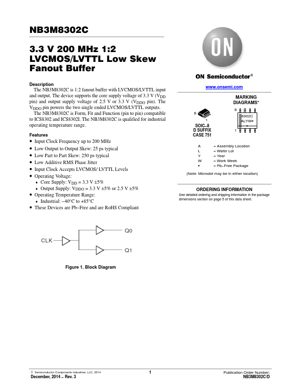
Figure 1. Block Diagram
© Semiconductor ponents Industries, LLC, 2014
December, 2014
- Rev. 3
Publication Order Number:...