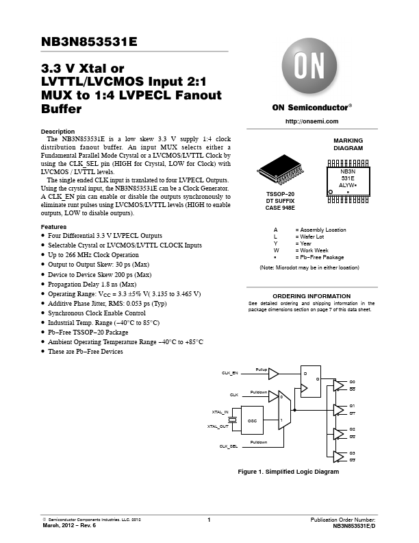
Datasheet4U Logo Datasheet4U.com

NB3N853531E - 3.3V Xtal or LVTTL/LVCMOS Input 2:1 MUX to 1:4 LVPECL Fanout Buffer

Datasheet Summary

Description

distribution fanout buffer.

An input MUX selects either a Fundamental Parallel Mode Crystal or a LVCMOS/LVTTL Clock by using the CLK_SEL pin (HIGH for Crystal, LOW for Clock) with LVCMOS / LVTTL levels.

Features

  • Four Differential 3.3 V LVPECL Outputs.
  • Selectable Crystal or LVCMOS/LVTTL CLOCK Inputs.
  • Up to 266 MHz Clock Operation.
  • Output to Output Skew: 30 ps (Max).
  • Device to Device Skew 200 ps (Max).
  • Propagation Delay 1.8 ns (Max).
  • Operating Range: VCC = 3.3 ±5% V( 3.135 to 3.465 V).
  • Additive Phase Jitter, RMS: 0.053 ps (Typ).
  • Synchronous Clock Enable Control.
  • Industrial Temp. Range (.
  • 40°C to 85°C).

📥 Download Datasheet

Datasheet preview – NB3N853531E

Datasheet Details

Part number NB3N853531E
Manufacturer ON Semiconductor
File Size 236.85 KB
Description 3.3V Xtal or LVTTL/LVCMOS Input 2:1 MUX to 1:4 LVPECL Fanout Buffer
Datasheet download datasheet NB3N853531E Datasheet
Additional preview pages of the NB3N853531E datasheet.
Other Datasheets by ON Semiconductor

Full PDF Text Transcription

Click to expand full text
NB3N853531E 3.3 V Xtal or LVTTL/LVCMOS Input 2:1 MUX to 1:4 LVPECL Fanout Buffer Description The NB3N853531E is a low skew 3.3 V supply 1:4 clock distribution fanout buffer. An input MUX selects either a Fundamental Parallel Mode Crystal or a LVCMOS/LVTTL Clock by using the CLK_SEL pin (HIGH for Crystal, LOW for Clock) with LVCMOS / LVTTL levels. The single ended CLK input is translated to four LVPECL Outputs. Using the crystal input, the NB3N853531E can be a Clock Generator. A CLK_EN pin can enable or disable the outputs synchronously to eliminate runt pulses using LVCMOS/LVTTL levels (HIGH to enable outputs, LOW to disable outputs). Features • Four Differential 3.
Published: |