NB3RL02
NB3RL02 is Low Phase-Noise Two-Channel Clock Fanout Buffer manufactured by onsemi.
Low Phase-Noise Two-Channel Clock Fanout Buffer
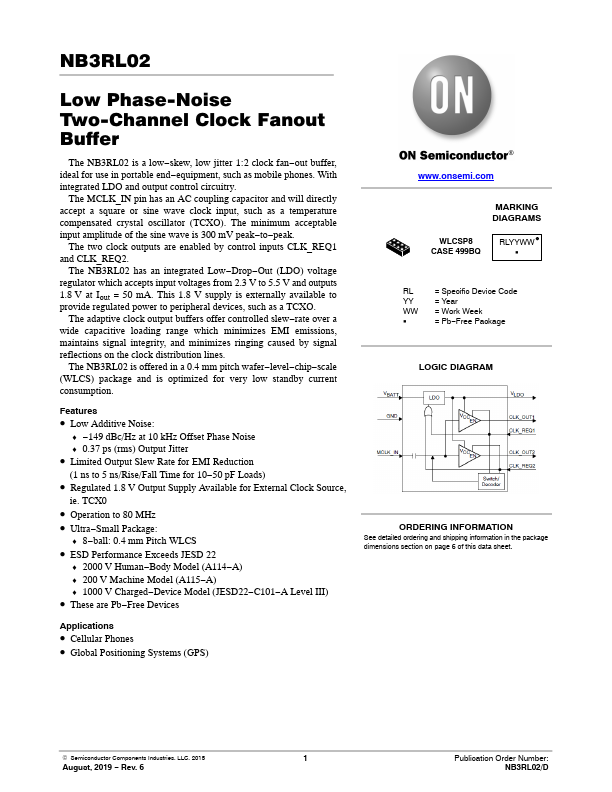
The NB3RL02 is a low- skew, low jitter 1:2 clock fan- out buffer, ideal for use in portable end- equipment, such as mobile phones. With integrated LDO and output control circuitry.
The MCLK_IN pin has an AC coupling capacitor and will directly accept a square or sine wave clock input, such as a temperature pensated crystal oscillator (TCXO). The minimum acceptable input amplitude of the sine wave is 300 m V peak- to- peak.
The two clock outputs are enabled by control inputs CLK_REQ1 and CLK_REQ2.
The NB3RL02 has an integrated Low- Drop- Out (LDO) voltage regulator which accepts input voltages from 2.3 V to 5.5 V and outputs 1.8 V at Iout = 50 m A. This 1.8 V supply is externally available to provide regulated power to peripheral devices, such as a TCXO.
The adaptive clock output buffers offer controlled slew- rate over a wide capacitive loading range which minimizes EMI emissions, maintains signal integrity, and minimizes ringing caused by signal reflections on the clock distribution lines.
The NB3RL02 is offered in a 0.4 mm pitch wafer- level- chip- scale (WLCS) package and is optimized for very low standby current consumption.
Features
- Low Additive Noise:
- - 149 d Bc/Hz at 10 k Hz Offset Phase Noise
- 0.37 ps (rms) Output Jitter
- Limited Output Slew Rate for EMI Reduction
(1 ns to 5 ns/Rise/Fall Time for 10- 50 p F Loads)
- Regulated 1.8 V Output Supply Available for External Clock Source, ie. TCX0
- Operation to 80 MHz
- Ultra- Small Package:
- 8- ball: 0.4 mm Pitch WLCS
- ESD Performance Exceeds JESD 22
- 2000 V Human- Body Model (A114- A)
- 200 V Machine Model (A115- A)
- 1000 V Charged- Device Model (JESD22- C101- A Level III)
- These are Pb- Free Devices
Applications
- Cellular Phones
- Global Positioning Systems (GPS)
.onsemi.
MARKING DIAGRAMS
WLCSP8 CASE 499BQ
RLYYWW G
= Specific Device...


