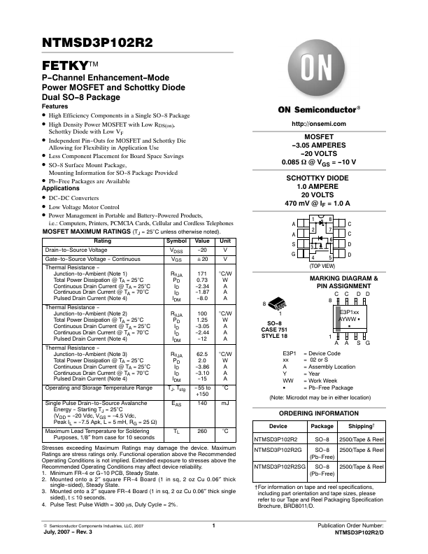
NTMSD3P102R2
NTMSD3P102R2 is P-Channel Enhancement-Mode Power MOSFET and Schottky Diode manufactured by onsemi.
Features
- ăHigh Efficiency ponents in a Single SO-8 Package
- ăHigh Density Power MOSFET with Low RDS(on),
Schottky Diode with Low VF
- ăIndependent Pin-Outs for MOSFET and Schottky Die
Allowing for Flexibility in Application Use
- ăLess ponent Placement for Board Space Savings
- ăSO-8 Surface Mount Package,
Mounting Information for SO-8 Package Provided
- ăPb-Free Packages are Available
Applications
- ăDC-DC Converters
- ăLow Voltage Motor Control
- ăPower Management in Portable and Battery-Powered Products, i.e.: puters, Printers, PCMCIA Cards, Cellular and Cordless Telephones
MOSFET MAXIMUM RATINGS (TJ = 25°C unless otherwise noted).
Rating
Symbol Value Unit
Drain-to-Source Voltage
Gate-to-Source Voltage
- Continuous
Thermal Resistance Junction-to-Ambient (Note 1) Total Power Dissipation @ TA = 25°C Continuous Drain Current @ TA = 25°C Continuous Drain Current @ TA = 70°C Pulsed Drain Current (Note 4)
VDSS
Rq JA PD ID ID IDM
-20 "20
171 0.73 -2.34 -1.87 -8.0
°C/W W A A A
Thermal Resistance
- Junction-to-Ambient (Note 2)
Total Power Dissipation @ TA = 25°C Continuous Drain Current @ TA = 25°C Continuous Drain Current @ TA = 70°C Pulsed Drain Current (Note 4)
Rq JA PD
ID IDM
100 1.25 -3.05 -2.44 -12
°C/W W A A A
Thermal Resistance Junction-to-Ambient (Note 3) Total Power Dissipation @ TA = 25°C Continuous Drain Current @ TA = 25°C Continuous Drain Current @ TA = 70°C Pulsed Drain Current (Note 4)
Operating and Storage Temperature Range
Rq JA PD ID ID IDM
TJ,...