NTMSD3P303R2
NTMSD3P303R2 is P-Channel Enhancement-Mode Power MOSFET and Schottky Diode manufactured by onsemi.
Features
- High Efficiency ponents in a Single SO- 8 Package
- High Density Power MOSFET with Low RDS(on),
Schottky Diode with Low VF
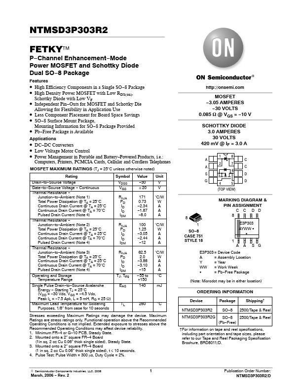
- Independent Pin- Outs for MOSFET and Schottky Die
Allowing for Flexibility in Application Use
- Less ponent Placement for Board Space Savings
- SO- 8 Surface Mount Package,
Mounting Information for SO- 8 Package Provided
- Pb- Free Package is Available
Applications
- DC- DC Converters
- Low Voltage Motor Control
- Power Management in Portable and Battery- Powered Products, i.e.: puters, Printers, PCMCIA Cards, Cellular and Cordless Telephones
MOSFET MAXIMUM RATINGS (TJ = 25°C unless otherwise noted)
Rating
Symbol Value Unit
Drain- to- Source Voltage Gate- to- Source Voltage
- Continuous Thermal Resistance
- Junction- to- Ambient (Note 1) Total Power Dissipation @ TA = 25°C Continuous Drain Current @ TA = 25°C PCuolnsteindu Dourasin Dr Cauinrr Cenutrr(e Nnot t@e 4T)A = 70°C Thermal Resistance
- Junction- to- Ambient (Note 2) Total Power Dissipation @ TA = 25°C Continuous Drain Current @ TA = 25°C Continuous Drain Current @ TA = 70°C Pulsed Drain Current (Note 4) Thermal Resistance
- Junction- to- Ambient (Note 3) Total Power Dissipation @ TA = 25°C Continuous Drain Current @ TA = 25°C Continuous Drain Current @ TA = 70°C Pulsed Drain Current (Note 4) Operating and Storage Temperature Range Single Pulse Drain- to- Source Avalanche Energy
- Starting TJ = 25°C (VDD =
- 30 Vdc, VGS =
- 4.5 Vdc, Peak IL =
- 7.5 Apk, L = 5 m H, RG = 25 W) Maximum Lead Temperature for Soldering Purposes, 1/8″ from case for 10 seconds
VDSS VGS RPq DJA ID ID IDM RPq DJA ID IDIDM RPq DJA ID ID IDM TJ, Tstg EAS
- 30 "20
171 0.73
- 2.34
- 1.87
- 8.0
°C/W W A A A
100 1.25
- 3.05
- 2.44
- 12
°C/W W A A...