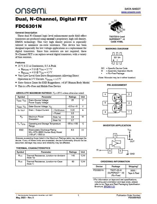
FDC6301N
Overview
These dual N-Channel logic level enhancement mode field effect transistors are produced using onsemi’s proprietary, high cell density, DMOS technology. This very high density process is especially tailored to minimize on-state resistance.
- 25 V, 0.22 A Continuous, 0.5 A Peak
- RDS(on) = 5 W @ VGS = 2.7 V
- RDS(on) = 4 W @ VGS = 4.5 V
- Very Low Level Gate Drive Requirements Allowing Direct Operation in 3 V Circuits. VGS(th) < 1.5 V
- Gate-Source Zener for ESD Ruggedness. >6 kV Human Body Model
- This is a Pb-Free and Halide Free Device