2SD661
Key Features
- 5 R0.9 R0.9
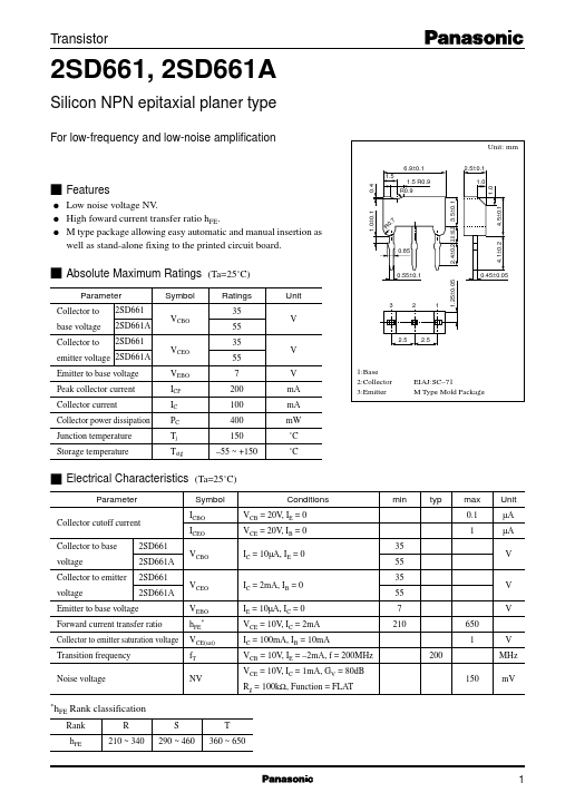
- 85 Parameter Collector to base voltage Collector to 2SD661 2SD661A 2SD661 Symbol VCBO VCEO VEBO ICP IC PC Tj Tstg Ratings 35 55 35 55 7 200 100 400 150 -55 ~ +150 Unit 3 2 1 V
- 5 2.5 emitter voltage 2SD661A Emitter to base voltage Peak collector current Collector current Collector power dissipation Junction temperature Storage temperature V V mA mA mW ˚C ˚C 1:Base 2:Collector 3:Emitter EIAJ:SC-71 M Type Mold Package s Electrical Characteristics Parameter Collector cutoff current Collector to base voltage Collector to emitter voltage 2SD661 2SD661A 2SD661 2SD661A (Ta=25˚C) Symbol ICBO ICEO VCBO VCEO VEBO hFE* VCE(sat) fT NV Conditions VCB = 20V, IE = 0 VCE = 20V, IB = 0 IC = 10µA, IE = 0 IC = 2mA, IB = 0 IE = 10µA, IC = 0 VCE = 10V, IC = 2mA IC = 100mA, IB = 10mA VCB = 10V, IE = -2mA, f = 200MHz VCE = 10V, IC = 1mA, GV = 80dB Rg = 100kΩ, Function = FLAT 200 150 35 55 35 55 7 210 650 1 V MHz mV min typ max 0.1 1 Unit µA µA V
- 25±0.05 s Absolute Maximum Ratings (Ta=25˚C)
- 55±0.1
- 45±0.05
- 1±0.2 Low noise voltage NV. High foward current transfer ratio hFE. M type package allowing easy automatic and manual insertion as well as stand-alone fixing to the printed circuit board.
- 0±0.1 R 0.
- 5±0.1 7 V V Emitter to base voltage Forward current transfer ratio Collector to emitter saturation voltage Transition frequency Noise voltage
- h FE Rank classification R 210 ~ 340 S 290 ~ 460 T 360 ~ 650 hFE Rank 1 Transistor PC - Ta