PI6CV304
PI6CV304 is 160 MHz Clock Buffers manufactured by Pericom Semiconductor.
Features
- -
- -
- -
- - 160 MHz operation Low noise, low skew: 150ps max Fast rise/fall time: 1.0ns typ. Fast propagation delay: 2.0ns typ. 5V I/O tolerant input Industrial temperature (- 40°C to 85°C) 3.3V power supply Packaging (Pb-free & Green available)
- 8-pin TSSOP (L)
- 8-pin SOIC (W)
Description
Peri’s PI6CV304 and PI6CV2304 are low-skew, low- noise, highspeed clock buffers and are ideal for puting, networking, and munication applications. Application examples include PCI(X) clock buffers in servers and workstations, PCI(X) Storage Area Network (SAN), and RAID controllers. They are used for networking and munications applications requiring 80 MHz for 10/100 Mbps Ethernet and 125 MHz for Gigabit networking clocks. To reduce EMI emission and power consumption, all outputs can be disabled to 3-state by asserting a low signal to the OE (Output Enable) pin. PI6CV2304 output impedance is 30-ohms. PI6CV304 output impedance is 20-ohms.
Applications
- 33 MHz PCI-to-133 MHz PCIX controllers
- 80 MHz for 10/100 Mbps Ethernet
- 125 MHz for Gigabit networking
- 155 MHz for Optical OC3/SDH/SONET
Function Table
Inputs CLK_IN X L H OE L H H Output Y[0:3] Z L H
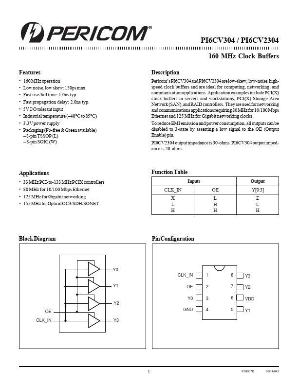
Block Diagram
Pin Configuration
Y0
CLK_IN
Y1
1 2 3 4
8 7 6 5
Y3 Y2 VDD Y1
OE Y0
Y2 OE CLK_IN Y3
PS8537D
09/14/043
PI6CV304 / PI6CV2304 160 MHz Clock Buffers 12345678901234567890123456789012123456789012345678901234567890121234567890123456789012345678901212345678901234567890123456789012123456789012
Pin Description
Pin # 1 2 3,5,7,8 4 6 Symbol CLK_IN OE Y[0- 3] GND VDD Type Input Input Output Ground Power Qty 1 1 4 1 1 5V Tolerant clock input Active High Output Enable. Y[0- 3] outputs will be 3- stated when OE is low LVCMOS level outputs Ground 3.3V power De s cription
Absolute Maximum Ratings (Above which the useful life may be impaired. For user...