PI6CVF857
PI6CVF857 is 1:10 PLL Clock Driver manufactured by Pericom Semiconductor.
Features
- Operating Frequency up to 220 MHz for PC3200 Registered DIMM applications
- Distributes one differential clock input pair to ten differential clock output pairs
- Inputs (CLK,CLK) and (FBIN,FBIN)
..
- Input PWRDWN:
Product Description
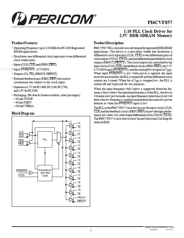
PI6CVF857 PLL clock device is developed for registered DDR DIMM applications. The device is a zero-delay buffer that distributes a differential clock input pair (CLK, CLK) to ten differential pairs of clock outputs (Y[0:9], Y[0:9]), and one differential pair feedback clock outputs (FBOUT,FBOUT) . The clock outputs are controlled by the input clocks (CLK, CLK), the feedback clocks (FBIN,FBIN), the 2.5V LVCMOS input (PWRDWN), and the Analog Power input (AVDD). When input PWRDWN is low while power is applied, the input receivers are disabled, the PLL is turned off, and the differential clock outputs are 3-stated. When the AVDD is strapped low, the PLL is turned off and bypassed for test purposes. When the input frequency falls below a suggested detection frequency that is below the operating frequency of the PLL, the device will enter a low power mode. An input frequency detection circuit will detect the low frequency condition and perform the same low power features as when the PWRDWN input is low. The PLL in the PI6CVF857 clock driver uses the input clocks (CLK, CLK) and the feedback clocks (FBIN,FBIN) to provide high-performance, low-skew, low-jitter output differential clocks (Y[0:9], Y[0:9]). The PI6CVF857 is also able to track Spread Spectrum Clocking for reduced EMI.
LVCMOS
- Outputs (Yx, Yx), (FBOUT, FBOUT)
- External feedback pins (FBIN,FBIN) are used to synchronize the outputs to the clock input
- Operates at 2.5V for PC1600, PC2100, PC2700, and 2.6V for PC3200
- Packaging (Pb-free & Green available, select packages):
- 48-pin TSSOP
- 40-pin TQFN
- 56-ball VFBGA
Block Diagram
Y0 Y0 Y1 Y1 Y2 Y2 Y3 Y3 Y4 Y4 Y5 Y5 Y6 Y6 Y7 Y7 Y8 Y8 Y9 Y9 FBOUT FBOUT
CLK CLK FBIN FBIN PLL
PWRDWN AVDD
Powerdown and Test...