PLL130-07
PLL130-07 is High Speed Translator Buffer to CMOS manufactured by PhaseLink Corporation.
FEATURES
CMOS output Selectable Drive capability (15p F or 30p F output load).
- Single AC coupled input (min. 100m V swing).
- Input range from DC to 200 MHz.
- 2.5V to 3.3V operation.
- Available in 8-Pin SOIC and 3x3mm QFN. ..
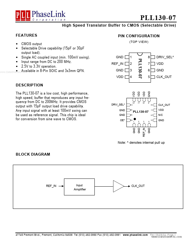
- - PIN CONFIGURATION
(TOP VIEW)
GND REF_IN GND VDD
1 2 3 4
8 7 6 5
DRIV_SEL^ VDD GND CLK_OUT
DESCRIPTION
The PLL130-07 is a low cost, high performance, high speed, buffer that reproduces any input frequency from DC to 200MHz. It provides CMOS output with 15p F output load drive capability. Any input signal with at least 100m V swing can be used as reference signal. This chip is ideal for conversion from sine wave to CMOS.
DRIV_SEL^ GND GND OE^
13 14 15 16
8 7 6 5
CLK_OUT VDD N/C GND
1 2 3 4
REF_IN
Note: ^ denotes internal pull up
BLOCK DIAGRAM
REF_IN
Input
Amplifier
CLK_OUT
47745 Fremont Blvd., Fremont, California 94538 Tel (510) 492-0990 Fax (510) 492-0991 .phaselink. Rev 09/09/04 Page 1
High Speed Translator Buffer to CMOS (Selectable Drive) PIN DESCRIPTION
Name
GND VDD DRIV_SEL
..
8pin SOIC Pin number
1,3,6 4,7 8 2 5 N/A
3x3mm QFN Pin number
1,2,4,5, 9,14,15 7,10,11,12 13 3 8...