PLL205-04
FEATURES
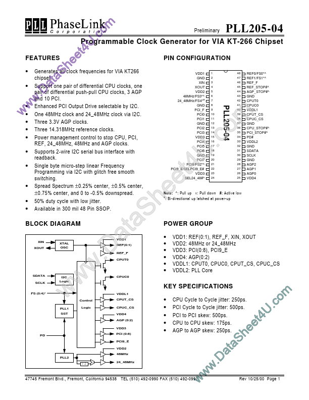
PIN CONFIGURATION e h
- Generates all clock frequencies for VIA KT266 S chipset. a t
- Support one pair of differential CPU clocks, one a pair of differential push-pull CPU clocks, 3 AGP .D and 10 PCI. w
- w Enhanced PCI Output Drive selectable by I2C. w- One 48MHz clock and 24_48MHz clock via I2C.
- -
- -
- -
- - Three 3.3V AGP clocks. Three 14.318MHz reference clocks. Power management control to stop CPU, PCI, REF, 24_48MHz, 48MHz and AGP clocks. Supports 2-wire I2C serial bus interface with readback. Single byte micro-step linear Frequency Programming via I2C with glitch free smooth switching. Spread Spectrum ± 0.25% center, ± 0.5% center, ± 0.75% center, and 0 to -0.5% downspread. 50% duty cycle with low jitter. Available in 300 mil 48 Pin SSOP.
BLOCK DIAGRAM
XIN XOUT XTAL OSC
SDATA SCLK
I2C Logic
FS (0:4)- m o .c U 4 t e e h S a t a .D w w w
9 10 11 12 13 14 15 16 17 18 19 20 21 22 23 24 40 39 38 37 36 35 34 33 32 31 30 29 28 27 26 25
VDD1 GND XIN XOUT VDD2...