9FGS9093 Overview
Key Specifications
Mount Type: Surface Mount
Pins: 24
Operating Voltage: 3.3 V
Max Voltage (typical range): 3.465 V
Key Features
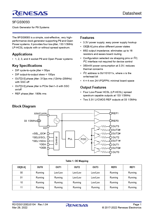
- 3 1.1 Pin Assignments
| Part | 9FGS9093 |
|---|---|
| Description | Clock Generator |
| Manufacturer | Renesas |
| Size | 615.56 KB |
Mount Type: Surface Mount
Pins: 24
Operating Voltage: 3.3 V
Max Voltage (typical range): 3.465 V
| Seller | Inventory | Price Breaks | Buy |
|---|---|---|---|
| VNN Services | 3821 | 1+ : 4.54 USD 10+ : 4.45 USD 100+ : 4.36 USD 1000+ : 4.27 USD |
View Offer |
| Aztech | 600 | 1+ : 14.68 USD | View Offer |
| Part Number | Manufacturer | Description |
|---|---|---|
| XR2206 | Exar | Monolithic Function Generator |
| AN97 | Maxim Integrated | Telephone Tone Generator |
| AN97 | Maxim Integrated | Telephone Tone Generator Requires No trimming |