RJK2054DPC
RJK2054DPC is N-Channel Power MOSFET manufactured by Renesas.
Features
- Low on-resistance RDS(on) = 0.075 Ω typ. (at ID = 8.5 A, VGS = 10 V, Ta = 25°C)
- Low drive current
- High density mounting REJ03G1868-0100 Rev.1.00 Dec 08, 2009
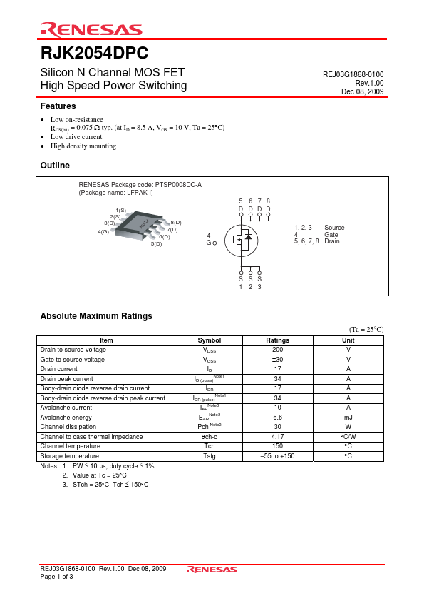
Outline
RENESAS Package code: PTSP0008DC-A (Package name: LFPAK-i)
1(S) 2(S) 3(S) 4(G)
5 6 7 8 D D D D
K2 05 4
8(D) 7(D) 6(D) 5(D)
4 G
1, 2, 3 Source 4 Gate 5, 6, 7, 8 Drain
S S S 1 2 3
.Data Sheet.co.kr
Absolute Maximum Ratings
(Ta = 25°C)
Item Drain to source voltage Gate to source voltage Drain current Drain peak current Body-drain diode reverse drain current Body-drain diode reverse drain peak current Avalanche current Avalanche energy Channel dissipation Channel to case thermal impedance Channel temperature Storage temperature Notes: 1. PW ≤ 10 μs, duty cycle ≤ 1% 2. Value at Tc = 25°C 3. STch = 25°C, Tch ≤ 150°C Symbol VDSS VGSS ID ID (pulse)Note1 IDR IDR (pulse)Note1 IAPNote3 EARNote3 Pch Note2 θch-c Tch Tstg Ratings 200 ±30 17 34 17 34 10 6.6 30 4.17 150
- 55 to +150 Unit V V A A A A A m J W °C/W °C °C
REJ03G1868-0100 Rev.1.00 Dec 08, 2009 Page 1 of 3
Datasheet pdf
- http://..net/
Electrical Characteristics
(Ta = 25°C)
Item Drain to source breakdown voltage Zero gate voltage drain current Gate to source leak current Gate to source cutoff voltage Static drain to source on state resistance Input capacitance Output capacitance Reverse transfer capacitance Turn-on delay time Rise time Turn-off delay time Fall time Total gate charge Gate to source charge Gate to drain charge Body-drain diode forward voltage Body-drain diode reverse recovery time Notes: 4. Pulse test Symbol V(BR)DSS IDSS IGSS VGS(off) RDS(on) Ciss Coss Crss td(on) tr td(off) tf Qg Qgs Qgd VDF trr Min 200
- - 2.5
- -
- -
- -
- -
- -
- -
- Typ
- -
- - 0.075 1700 180 37 21 13 40 13 27.3 8.6 7.8 0.82 110 Max
- 1 ±1 4.5 0.098
- -
- -
- -
- -
- -...