The following content is an automatically extracted verbatim text
from the original manufacturer datasheet and is provided for reference purposes only.
View original datasheet text
Preliminary Datasheet
RJK5030DPP-M0
Silicon N Channel MOS FET High Speed Power Switching
Features
Low on-state resistance RDS(on) = 1.3 typ. (at ID = 2 A, VGS = 10 V, Ta = 25C) High speed switching R07DS0227EJ0100 Rev.1.00 Dec 14, 2010
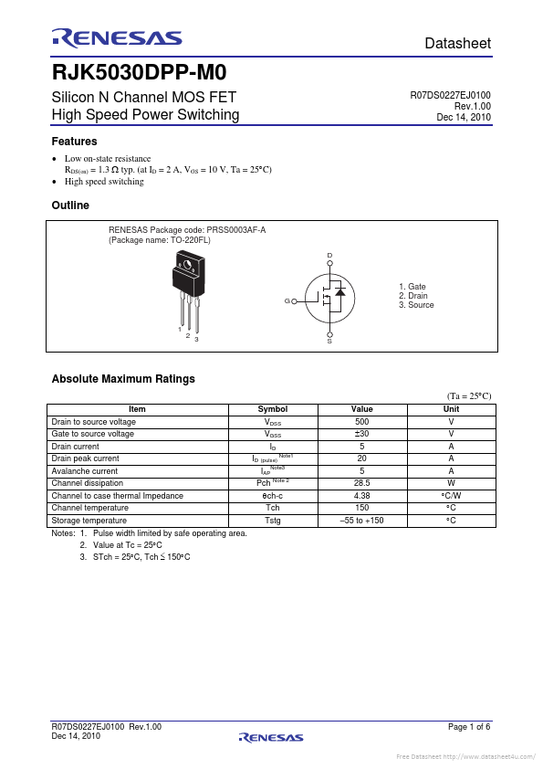
Outline
RENESAS Package code: PRSS0003AF-A (Package name: TO-220FL)
D
G
1. Gate 2. Drain 3. Source
1
2 3
S
Absolute Maximum Ratings
(Ta = 25C)
Item Drain to source voltage Gate to source voltage Drain current Drain peak current Avalanche current Channel dissipation Channel to case thermal Impedance Channel temperature Storage temperature Notes: 1. Pulse width limited by safe operating area. 2. Value at Tc = 25C 3. STch = 25C, Tch 150C Symbol VDSS VGSS ID ID (pulse) Note3 IAP Pch Note 2 ch-c Tch Tstg
Note1
Value 500 30 5 20 5 28.5 4.