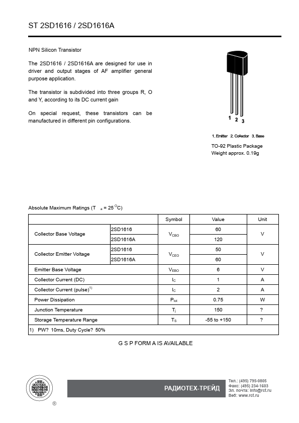
ABSOLUTE MAXIMUM RATINGS
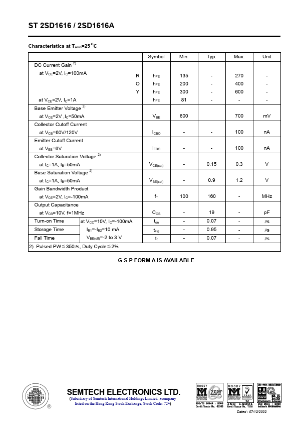
(T a = 25 OC) Collector Base Voltage 2SD1616 2SD1616A Collector Emitter Voltage 2SD1616 2SD1616A Emitter Base Voltage Collector Current (DC) Collector Current (pulse)1) Power Dissipation Junction Temperature Storage Temperature Range 1) PW? 10ms, Duty Cycle? 50% Symbol VCBO VCEO VEBO IC IC Ptot Tj TS G S P FORM A IS AVAILABLE Value 60 120 50 60 6 1 2 0.75 150 -55 to +150 Unit V V V A A W ? ? РАДИОТЕХ-ТРЕЙД Тел.: (495) 795-0805 Факс: (495) 234-1603 Эл. почта: info@rct.ru Веб: ® ST 2SD1616 / 2SD1616A Characteristics at Tamb=25 OC DC Current Gain 2) at VCE=2V, IC=100mA R O Y at VCE=2V, IC=1A Base Emitter Voltage 2) at VCE=2V ,IC=50mA Collector Cutoff Current at VCB=60V/120V Emitter Cutoff Current at VEB=6V Collector Saturation Voltage 2) at IC=1A, IB=50mA Base Saturation Voltage 2) at IC=1A, IB=50mA Gain Bandwidth Product at VCE=2V, IC=-100mA Output Capacitance at VCB=10V, f=1MHz Turn-on Time at VCC=10V, IC=-100mA Storage Time IB1=-IB2=10 mA Fall Time VBE(off)=-2 to 3 V 2) Pulsed PW≦350µs, Duty Cycle≦2% Symbol hFE hFE hFE hFE VBE ICBO IEBO VCE(sat) VBE(sat) fT COB ton tstg tf Min. Semtech Corporation