M59PW1282 Overview
7 Address Inputs (A0-A21) . Data Inputs/Outputs (DQ0-DQ7). Data Inputs/Outputs (DQ8-DQ15).
M59PW1282 Key Features
- MASK-ROM PIN-OUT PATIBLE
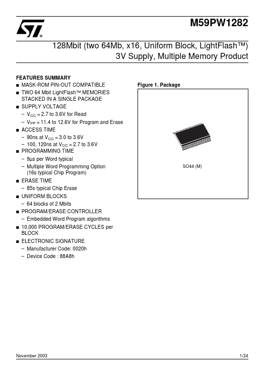
- Figure 1. Package
- VCC = 2.7 to 3.6V for Read
- VPP = 11.4 to 12.6V for Program and Erase
- 90ns at VCC = 3.0 to 3.6V
- 100, 120ns at VCC = 2.7 to 3.6V PROGRAMMING TIME
- 9µs per Word typical
- Multiple Word Programming Option (16s typical Chip Program)
- 85s typical Chip Erase UNIFORM BLOCKS
- 64 blocks of 2 Mbits PROGRAM/ERASE CONTROLLER