Datasheet Details
| Part number | STB3NC60 |
|---|---|
| Manufacturer | STMicroelectronics |
| File Size | 173.18 KB |
| Description | N-CHANNEL Power MOSFET |
| Datasheet | STB3NC60_STMicroelectronics.pdf |
|
|
|
Overview: ® STB3NC60 N - CHANNEL 600V - 3.3Ω - 3A - D2PAK/I2PAK PowerMESH™ ΙΙ MOSFET TYPE STB3NC60 ν ν ν ν ν VDSS 600 V R DS(on) < 3.6 Ω ID 3A TYPICAL RDS(on) = 3.
| Part number | STB3NC60 |
|---|---|
| Manufacturer | STMicroelectronics |
| File Size | 173.18 KB |
| Description | N-CHANNEL Power MOSFET |
| Datasheet | STB3NC60_STMicroelectronics.pdf |
|
|
|
The PowerMESH™ II is the evolution of the first generation of MESH OVERLAY™ .
The layout refinements introduced greatly improve the Ron*area figure of merit while keeping the device at the leading edge for what concerns switching speed, gate charge and ruggedness.
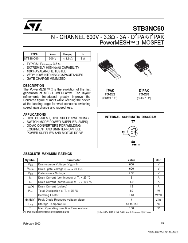
APPLICATIONS HIGH CURRENT, HIGH SPEED SWITCHING ν SWITCH MODE POWER SUPPLIES (SMPS) ν DC-AC CONVERTERS FOR WELDING EQUIPMENT AND UNINTERRUPTIBLE POWER SUPPLIES AND MOTOR DRIVE ν I2PAK TO-262 (Suffix "-1") D2PAK TO-263 (Suffix "T4") INTERNAL SCHEMATIC DIAGRAM ABSOLUTE MAXIMUM RATINGS Symbol V DS VDGR V GS ID ID I DM ( • ) P tot dv/dt( 1 ) T stg Tj Parameter Drain-source Voltage (V GS = 0) Drain- gate Voltage (R GS = 20 k Ω ) Gate-source Voltage Drain Current (continuous) at T c = 25 o C Drain Current (continuous) at T c = 100 C Drain Current (pulsed) Total Dissipation at T c = 25 o C Derating Factor Peak Diode Recovery voltage slope Storage Temperature Max.
| Part Number | Description |
|---|---|
| STB3NC90Z | N-CHANNEL Power MOSFET |
| STB3NA60-1 | N-CHANNEL Power MOSFET |
| STB3NA80 | N-CHANNEL Power MOSFET |
| STB3NB60 | N-CHANNEL Power MOSFET |
| STB3NK60Z | N-CHANNEL Power MOSFET |
| STB300NH02L | N-CHANNEL Power MOSFET |
| STB3015L | N-CHANNEL Power MOSFET |
| STB3020L | N-CHANNEL Power MOSFET |
| STB30N10 | N-CHANNEL Power MOSFET |
| STB30NE06L | N-CHANNEL Power MOSFET |