STMicroelectronics 2N1711
The 2N1711 is also used to advantage in amplifiers where low noise is an important factor. 2N1613 2N1711 SWITCHES AND UNIVERSAL AMPLIFIERS DESCRIPTION The 2N1613 and 2N1711 are silicon planar epitaxial NPN transistors in Jedec TO-39 metal case.| Part No. | 2N1711 |
|---|---|
| Datasheet | 2N1711 Download |
| Manufacturer |  STMicroelectronics |
| Description | SWITCHES AND UNIVERSAL AMPLIFIERS |
| Buy | Stock & Price |
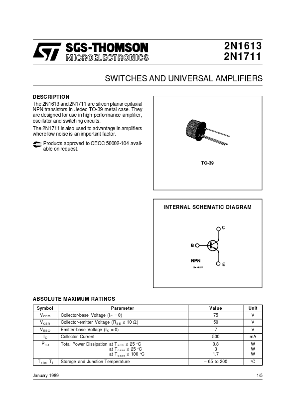
ABSOLUTE MAXIMUM RATINGS
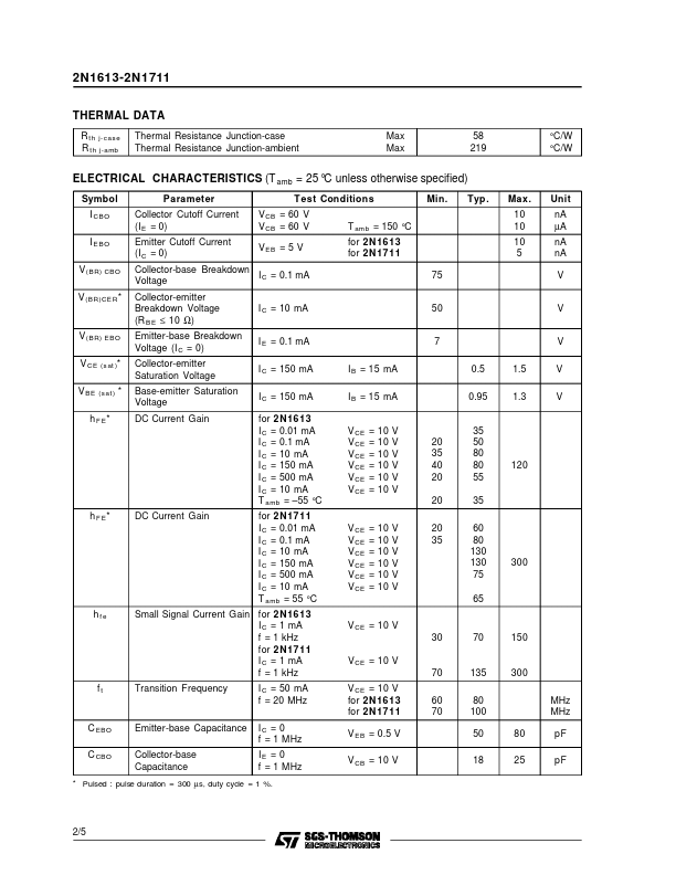
Symbol V CBO V CER V EBO IC Pt o t Parameter Collector-base Voltage (I E = 0) Collector-emitter Voltage (R BE ≤ 10 Ω ) Emitter-base Voltage (I C = 0) Collector Current Total Power Dissipation at T amb ≤ 25 °C at T c as e ≤ 25 °C at T c as e ≤ 100 °C Storage and Junction Temperature Value 75 50 7 500 0.8 3 1.7 – 65 to 200 Unit V V V mA W W W °C 1/5 T s t g, T j January 1989 2N1613-2N1711 THERMAL DATA R t h j- cas e R t h j-amb Thermal Resistance Junction-case Thermal Resistance Junction-ambient Max Max 58 219 °C/W °C/WELECTRICAL CHARACTERISTICS
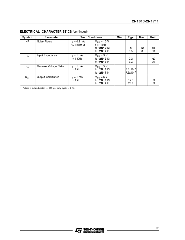
(T amb = 25 °C unless otherwise specified) Symbol I CBO I E BO V ( BR) CBO Parameter Collector Cutoff Current (I E = 0) Emitter Cutoff Current (I C = 0) Test Conditions V CB = 60 V V CB = 60 V V EB = 5 V T am b = 150 °C for 2N 16 13 for 2N 17 11 Min. Typ. Max. 10 10 10 5 Unit nA µA nA nA V Collector-base Breakdown I C = 0.1 mA Voltage Collector-emitter Breakdown Voltage (R B E ≤ 10 Ω) Emitter-base Breakdown Voltage (I C...