Datasheet Details
| Part number | P4NC50 |
|---|---|
| Manufacturer | STMicroelectronics |
| File Size | 322.25 KB |
| Description | STP4NC50 |
| Datasheet | P4NC50-STMicroelectronics.pdf |
|
|
|
Overview: STP4NC50 STP4NC50FP N-CHANNEL 500V - 2.2Ω - 3.5A TO-220/TO-220FP PowerMesh™II MOSFET TYPE VDSS RDS(on) ID STP4NC50 500 V < 2.7 Ω 3.5 A STP4NC50FP 500 V < 2.7 Ω 3.5 A s TYPICAL RDS(on) = 2.
| Part number | P4NC50 |
|---|---|
| Manufacturer | STMicroelectronics |
| File Size | 322.25 KB |
| Description | STP4NC50 |
| Datasheet | P4NC50-STMicroelectronics.pdf |
|
|
|
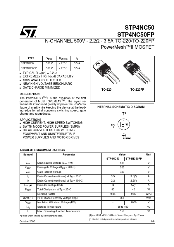
The PowerMESH™II is the evolution of the first generation of MESH OVERLAY™.
The layout re- finements introduced greatly improve the Ron*area figure of merit while keeping the device at the leading edge for what concerns switching speed, gate charge and ruggedness.
APPLICATIONS s HIGH CURRENT, HIGH SPEED SWITCHING s SWITH MODE POWER SUPPLIES (SMPS) s DC-AC CONVERTERS FOR WELDING EQUIPMENT AND UNINTERRUPTIBLE POWER SUPPLIES AND MOTOR DRIVES 3 2 1 TO-220 3 2 1 TO-220FP INTERNAL SCHEMATIC DIAGRAM ABSOLUTE MAXIMUM RATINGS Symbol Parameter VDS Drain-source Voltage (VGS = 0) VDGR Drain-gate Voltage (RGS = 20 kΩ) VGS Gate- source Voltage ID Drain Current (continuos) at TC = 25°C ID Drain Current (continuos) at TC = 100°C IDM (q) Drain Current (pulsed) PTOT Total Dissipation at TC = 25°C Derating Factor dv/dt (1) Peak Diode Recovery voltage slope VISO Insulation Withstand Voltage (DC) Tstg Storage Temperature Tj Max.
| Part Number | Description |
|---|---|
| P4NC60AFP | N-CHANNEL MOSFET |
| P4N150 | N-CHANNEL MOSFET |
| P4N20 | N-channel Power MOSFET |
| P4NA60FI | STP4NA60FI |
| P4NB50 | N-CHANNEL MOSFET |
| P4NB80 | STP4NB80 |
| P4NB80FP | STP4NB80FP |
| P4NK50Z | STP4NK50Z |
| P4NK60Z | STP4NK60Z |
| P4NK80Z | STP4NK80Z |