Using the latest high voltage MESH OVERLAY™ process, STMicroelectronics has designed an advanced family of power MOSFETs with outstanding performance.
Key Features
OF GATE-TO-SOURCE ZENER DIODES
The built-in back-to-back Zener diodes have specifically been designed to enhance not only the device’s ESD capability, but also to make them safely absorb possible voltage transients that may occasionally be applied from gate to source. In this respect the Zener voltage is appropriate to achieve an efficient and cost-effective intervention to protect the device’s integrity. These integrated Zener diodes thus avoid the usage of external components. 3/10
STD3PS25.
Full PDF Text Transcription for STD3PS25 (Reference)
Note: Below is a high-fidelity text extraction (approx. 800 characters) for
STD3PS25. For precise diagrams, tables, and layout, please refer to the original PDF.
View original datasheet text
STD3PS25 - STD3PS25-1
P-CHANNEL 250V - 2.1Ω - 3A DPAK/IPAK MESH OVERLAY™ MOSFET
TYPE
VDSS
RDS(on)
ID
STD3PS25 STD3PS25-1
250 V 250 V
< 2.8 Ω < 2.8 Ω
3A 3A
s TYPICAL RDS(on) = 2.1Ω s 100% AVALANCHE TESTED s APPLICATION ORIENTED
CHARACTERIZATION s STANDARD OUTLINE FOR EASY
AUTOMATED SURFACE MOUNT ASSEMBLY s GATE-SOURCE ZENER DIODE
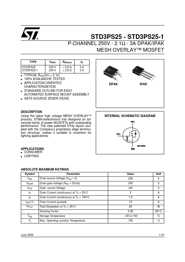
3 1
DPAK
IPAK
3
2 1
DESCRIPTION
Using the latest high voltage MESH OVERLAY™ process, STMicroelectronics has designed an advanced family of power MOSFETs with outstanding performance. The new patented STrip layout coupled with the Company’s proprietary edge termination structure, makes it suitable in coverters for lighting applications.