K7J163682B Description
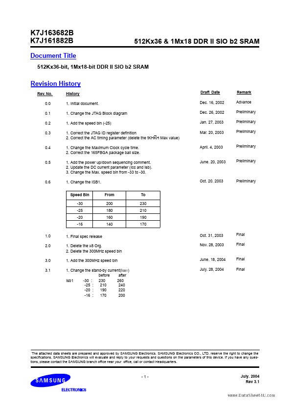
Document Title 512Kx36 & 1Mx18 DDR II SIO b2 SRAM 512Kx36-bit, 1Mx18-bit DDR II SIO b2 SRAM Revision History Rev. 0.0 0.1 0.2 0.3 History 1. Change the JTAG Block diagram.
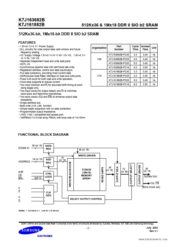
K7J163682B Key Features
- 1.8V+0.1V/-0.1V Power Supply
- DLL circuitry for wide output data valid window and future freguency scaling
- Separate independent read and write data ports
- HSTL I/O
- Synchronous pipeline read with self timed late write
- Registered address, control and data input/output
- Full data coherency, providing most current data
- DDR(Double Data Rate) Interface on read and write ports
- Fixed 2-bit burst for both read and write operation
- Clock-stop supports to reduce current