K7J321882M Description
on page 2 and add HSTL I/O ment 6. Deleted R/W control pin description on page 2 1. Update current characteristics in DC.
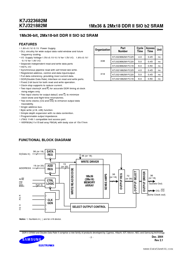
K7J321882M Key Features
- 1.8V+0.1V/-0.1V Power Supply
- DLL circuitry for wide output data valid window and future freguency scaling
- Separate independent read and write data ports
- HSTL I/O
- Synchronous pipeline read with self timed late write
- Registered address, control and data input/output
- Full data coherency, providing most current data
- DDR(Double Data Rate) Interface on read and write ports
- Fixed 2-bit burst for both read and write operation
- Clock-stop supports to reduce current