K7J641882M Description
2Mx36 & 4Mx18 DDR II SIO b2 SRAM 72Mb M-die DDRII SRAM Specification 165 FBGA with Pb & Pb-Free (RoHS pliant) INFORMATION IN THIS DOCUMENT IS PROVIDED IN RELATION TO SAMSUNG PRODUCTS, AND IS SUBJECT TO CHANGE WITHOUT NOTICE. NOTHING IN THIS DOCUMENT SHALL BE CONSTRUED AS GRANTING ANY LICENSE, EXPRESS OR IMPLIED, BY ESTOPPEL OR OTHERWISE, TO ANY INTELLECTUAL PROPERTY RIGHTS IN SAMSUNG PRODUCTS OR TECHNOLOGY. ALL...
K7J641882M Key Features
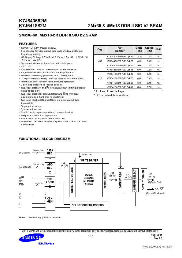
- 1.8V+0.1V/-0.1V Power Supply
- DLL circuitry for wide output data valid window and future freguency scaling
- Separate independent read and write data ports
- HSTL I/O
- Synchronous pipeline read with self timed late write
- Registered address, control and data input/output
- Full data coherency, providing most current data
- DDR(Double Data Rate) Interface on read and write ports
- Fixed 2-bit burst for both read and write operation
- Clock-stop supports to reduce current
K7J641882M Applications
- Samsung Electronics reserves the right to change products or specification without notice