The following content is an automatically extracted verbatim text
from the original manufacturer datasheet and is provided for reference purposes only.
View original datasheet text
Ordering number :EN5847
P-Channel Silicon MOS FET
FW113
S/W Load Applications
Features
· 4V drive. · Low ON resistance.
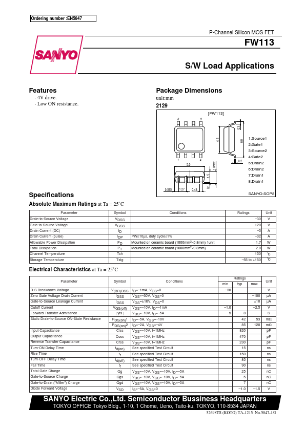
Package Dimensions
unit:mm 2129
[FW113] 85
0.1 1.5 1.8max 4.4 0.3 6.0
Specifications
Absolute Maximum Ratings at Ta = 25˚C
1 5.0
4
0.595 1.27 0.43
1:Source1 2:Gate1 3:Source2 4:Gate2 0.2 5:Drain2 6:Drain2 7:Drain1 8:Drain1
SANYO:SOP8
Parameter Drain-to-Source Voltage Gate-to-Source Voltage Drain Current (DC) Drain Current (pulse) Allowable Power Dissipation Total Dissipation Channel Temperature Storage Temperature
Symbol
VDSS VGSS
ID IDP PD PT Tch
Tstg
Conditions
PW≤10µs, duty cycle≤1% Mounted on ceramic board (1000mm2×0.8mm) 1unit Mounted on ceramic board (1000mm2×0.8mm)
Ratings –30 ±20 –5 –32 1.7 2.