2N6354
Description
SavantIC Semiconductor Product Specification Silicon NPN Power Transistors DESCRIPTION ·With TO-3 package ·Excellent safe operating area ·Fast switching speed ·Low collector saturation voltage ·Hig...
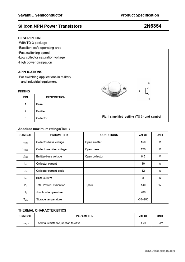
SavantIC Semiconductor Product Specification Silicon NPN Power Transistors DESCRIPTION ·With TO-3 package ·Excellent safe operating area ·Fast switching speed ·Low collector saturation voltage ·Hig...
| Part Number | Manufacturer | Description |
|---|---|---|
| 2N6354 | RCA | Power Transistor |
| 2N6351 | UNITRODE | Power NPN Transistor |
| 2N6353 | UNITRODE | Power NPN Darlingtons |
| 2N6356 | Inchange Semiconductor | NPN Transistor |
| 2N6350 | Microsemi | NPN DARLINGTON POWER SILICON TRANSISTOR |
| 2N6350 | UNITRODE | Power NPN Transistor |
| 2N6352 | UNITRODE | Power NPN Transistor |
| 2N6351 | VPT Components | NPN Darlington Power Silicon Transistor |
| 2N6358 | Inchange Semiconductor | NPN Transistor |
| 2N6353 | VPT Components | NPN Darlington Power Silicon Transistor |