2SB1063 Overview
Description
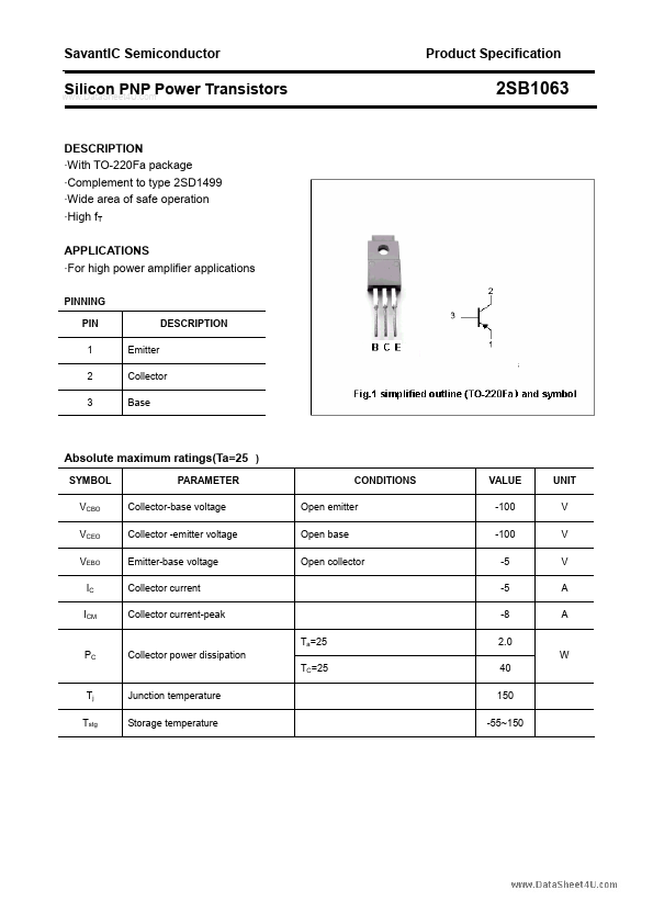
With TO-220Fa package - Complement to type 2SD1499 - Wide area of safe operation - High fT APPLICATIONS - For high power amplifier applications PINNING PIN 1 2 3 Emitter Collector Base DESCRIPTION SYMBOL VCBO VCEO VEBO IC ICM PARAMETER Collector-base voltage Collector -emitter voltage Emitter-base voltage Collector current Collector current-peak Ta=25 PC Collector power dissipation TC=25 Tj Tstg Junction temperature Storage temperature 40 150 -55~150 CONDITIONS Open emitter Open base Open collector VALUE -100 -100 -5 -5 -8 2.0 W UNIT V V V A A SavantIC Semiconductor Product Specification Silicon PNP Power Transistors CHARACTERISTICS Tj=25 unless otherwise specified PARAMETER Collector-emitter saturation voltage Base-emitter on voltage Collector cut-off current Emitter cut-off current DC current gain DC current gain DC current gain Transition frequency Collector output capacitance CONDITIONS IC=-3A ;IB=-0.3A IC=-3A ; VCE=-5V VCB=-100V; IE=0 VEB=-3V; IC=0 IC=-20mA ; VCE=-5V IC=-1A ; VCE=-5V IC=-3A ; VCE=-5V IC=-0.5A ; VCE=-5V IE=0 ; VCB=-10V; f=1MHz 20 40 20 MIN 2SB1063 SYMBOL VCEsat VBE ICBO IEBO hFE-1 hFE-2 hFE-3 fT COB TYP. MAX -2.0 -1.8 -50 -50 UNIT V V µA µA 200 20 170 MHz pF hFE-2 Classifications R 40-80 Q 60-120 P 100-200 2 SavantIC Semiconductor Product Specification Silicon PNP Power Transistors PACKAGE OUTLINE 2SB1063 Fig.2 Outline dimensions (unindicated tolerance: ±0.15 mm) 3.