2SC1815W
Description
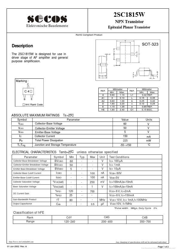
The 2SC1815W is designed for use in driver stage of AF amplifier and general purpose amplificaion.
REF. A A1 A2 D E HE
Min. 0.80 0 0.80 1.80 1.15 1.80
Millimeter
Max. 1.10 0.10 1.00 2.20 1.35 2.40
REF. L1 L b c e Q1
Min. Max. 0.42 REF. 0.15 0.35 0.25 0.40 0.10 0.25 0.65 REF. 0.15 BSC.
Millimeter
ABSOLUTE MAXIMUM RATINGS
Symbol VCBO VCEO VEBO Collector-Base Voltage
Ta=25o C
Parameter Value 60 50 5 150 225 -55~+150 Units V V V m A m W
IC PD TJ,Tstg
Collector-Emitter Voltage Emitter-Base Voltage Collector Current Total Power Dissipation Junction and Storage Temperature o
ELECTRICAL CHARACTERISTICS Tamb=25 C unless otherwise specified
Parameter
Collector-Base Breakdown Voltage Collector-Emitter Breakdown Voltage Emitter-Base Breakdown Voltage Collector-Base Cutoff Current Emitter-Base Cutoff Current Collector Saturation Voltage Base Saturation Voltage DC Current Gain Gain-Bandwidth Product Output Capacitance
Symbol BVCBO BVCEO BVEBO I CBO I EBO
- VCE(sat)
-...