DESCRIPTION
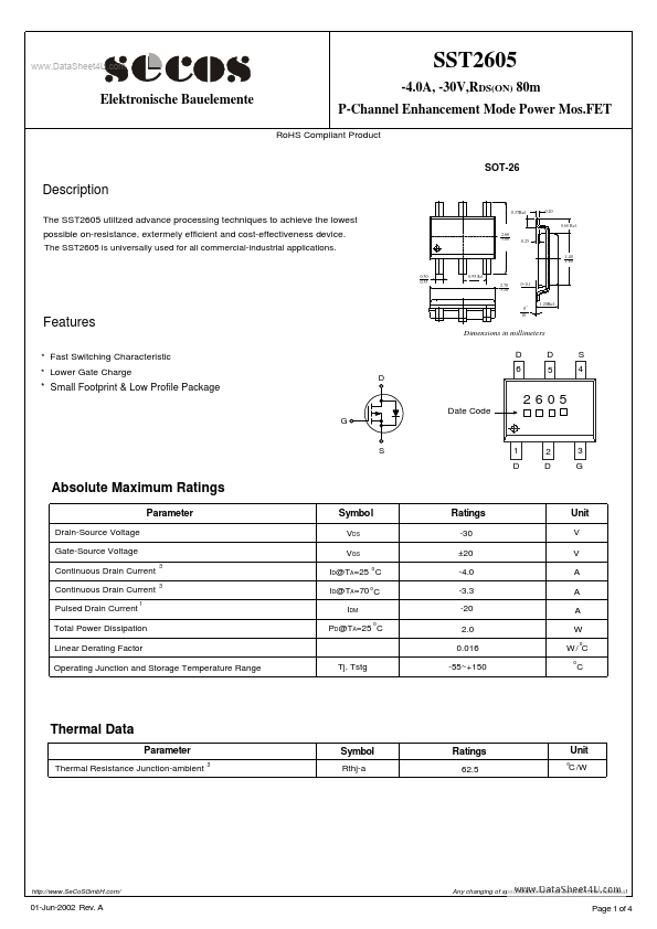
0.37Ref. 0.20 0.60 Ref. 2.60 3.00 0.25 1.40 1.80 0.30 0.55 0.95 Ref. 2.70 3.10 0~0.1 FEATURES
* Fast Switching Characteristic * Lower Gate Charge D 0 o 10 o 1.20Ref. Dimensions in millimeters D 6 D 5 S 4 * Small Footprint & Low Profile Package 2605 Date Code G S 1 D 2 D 3 G ABSOLUTE MAXIMUM RATINGS
Parameter Drain-Source Voltage Gate-Source Voltage Continuous Drain Current Continuous Drain Current Pulsed Drain Current 1 3 Symbol VDS VGS ID@TA=25 C ID@TA=70 C IDM PD@TA=25 C o o o Ratings -30 ±20 -4.0 -3.3 -20 2.0 0.016 Unit V V A A A W W/ C o o 3 Total Power Dissipation Linear Derating Factor Operating Junction and Storage Temperature Range Tj, Tstg -55~+150 C Thermal Data Parameter Thermal Resistance Junction-ambient 3 Symbol Rthj-a Ratings 62.5 o Unit C /W Any changing of specification will not be informed individual 01-Jun-2002 Rev. A Page 1 of 4 SST2605 -4.0A, -30V,RDS(ON) 80m£[ P-Channel Enhancement Mode Power Mos.FET Elektronische Bauelemente ELECTRICAL CHARACTERISTICS
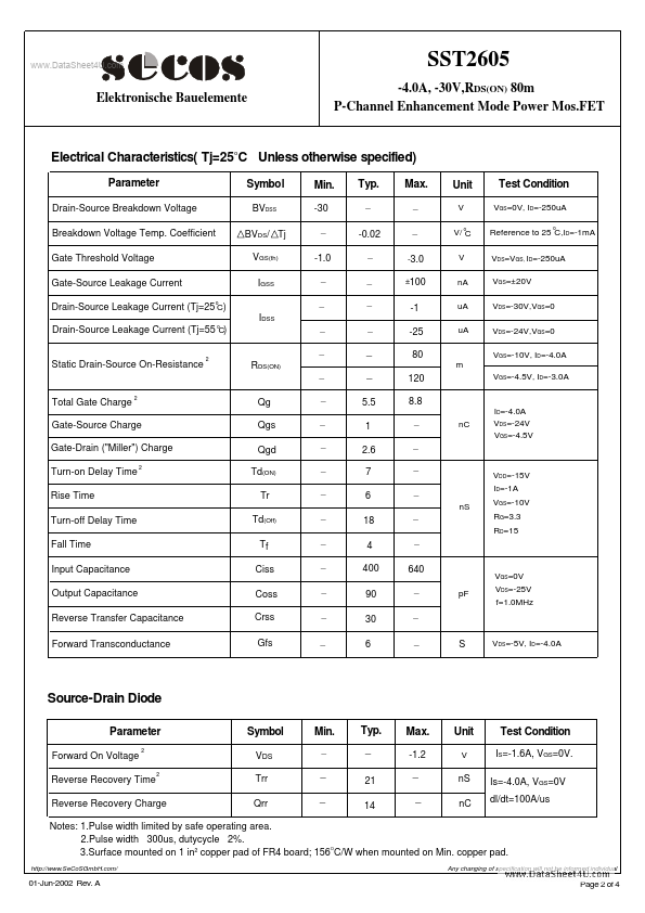
( Tj=25 C Unless otherwise specified) Parameter Drain-Source Breakdown Voltage Breakdown Voltage Temp. SeCoS Halbleitertechnologie GmbH